Printed Circuit Board Production: How the Process Works

Modern electronics depend on printed circuit board production because it creates a repeatable way to route electrical connections across a compact board. Before PCB’s became standard, many electronic devices relied on point-to-point wiring, with components connected manually using individual wires.

That approach worked, but it became increasingly difficult to manage as circuits grew more complex. Printed circuit boards changed the process by replacing much of that manual wiring with precisely defined conductive paths built directly into the board.

What Does “Printed” Mean?

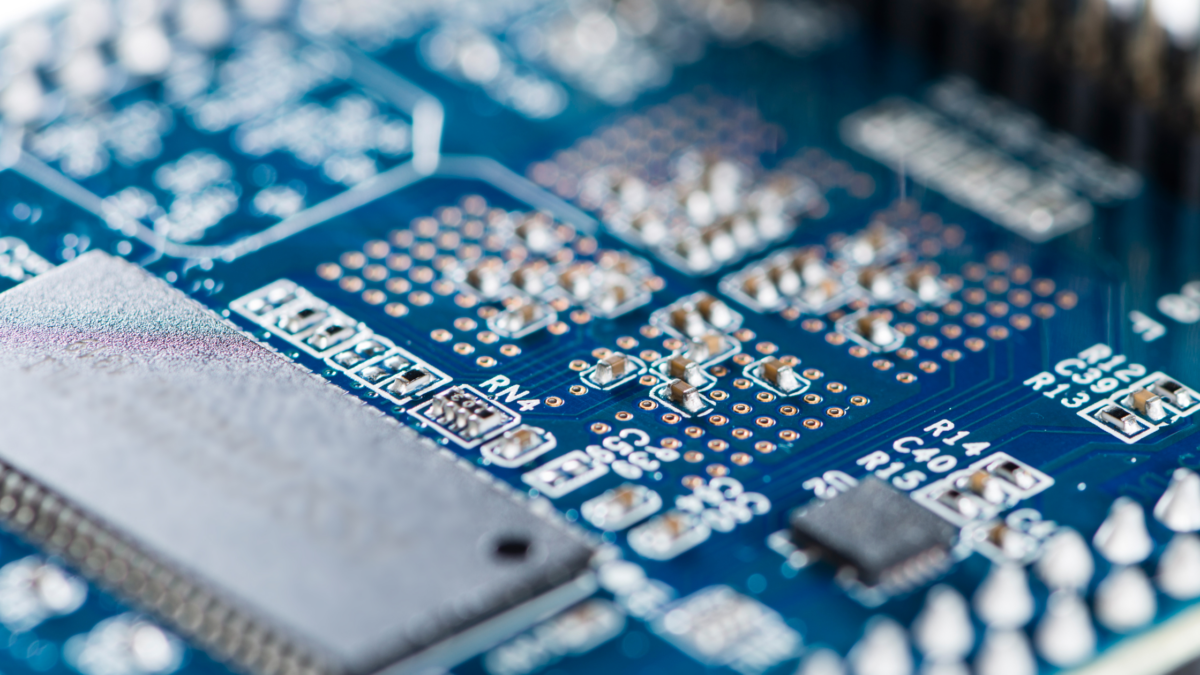
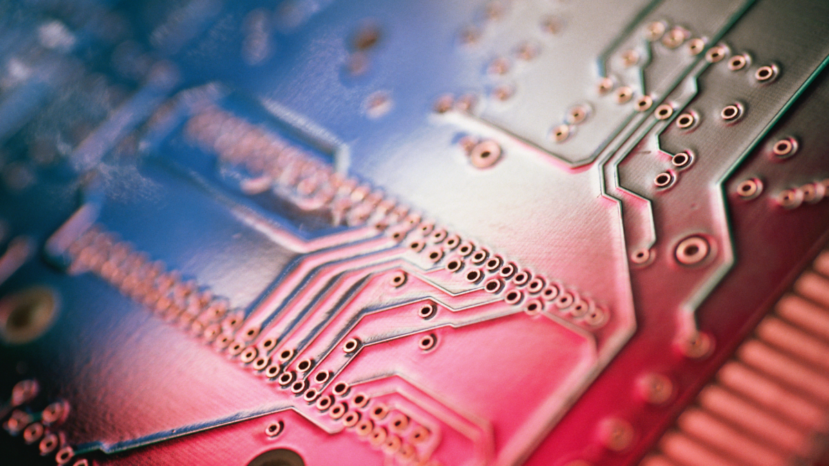
The word “printed” can be a little misleading. In conventional PCB fabrication, copper traces are not simply printed onto the board with ink. Instead, a circuit pattern is transferred onto copper-clad laminate using imaging and resist materials.

Unwanted copper is then removed through an etching process, leaving behind the conductive traces, pads, and other features required by the design.

That patterned copper is what gives a PCB its name. This process helps make printed circuit board production more consistent by allowing complex electrical pathways to be reproduced accurately from board to board.

How Printed Circuit Board Production Works

Printed circuit board production begins with the electronic design and manufacturing files that define how the board should be built. These files provide information about copper layers, drill locations, solder mask openings, and other features.

A simplified fabrication process may include:

  1. Preparing the laminate: Copper foil is bonded to an insulating substrate that provides structural support.
  2. Imaging the circuit pattern: A photosensitive resist is applied and exposed according to the PCB design.
  3. Etching the copper: Unprotected copper is removed, leaving the intended conductive traces behind.
  4. Drilling and plating: Holes may be drilled for vias, through-hole components, and connections between layers.
  5. Building additional layers: Multilayer PCBs repeat several of these processes before the layers are laminated together.

Manufacturing data often includes Gerber and drill files. Gerber files contain detailed layer information used during PCB fabrication. They should not be confused with 3D models of the finished board.

Solder Mask, Markings, and Surface Finish

After the copper circuitry has been created, several additional features help prepare the bare board for assembly.

These commonly include:

  • Solder mask: Protects copper and helps control where solder can make contact.
  • Silkscreen markings: Identify components, polarity, reference designators, and other important information.
  • Surface finish: Protects exposed copper pads while providing a suitable surface for soldering components.

Together, these finishing steps help make it easier to assemble while supporting consistent electrical connections.

Where PCB Assembly Begins

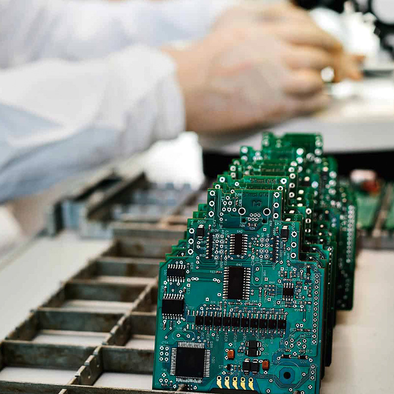
Once the bare PCB has been fabricated, the component assembly process can begin. This is the stage where a board starts becoming a functional electronic product.
printed circuit board production Nova

We provide printed circuit board production services that include surface mount, through-hole, and mixed-technology assemblies.

Depending on the design, the assembly process may involve:

  • Applying solder paste to designated surface mount pads
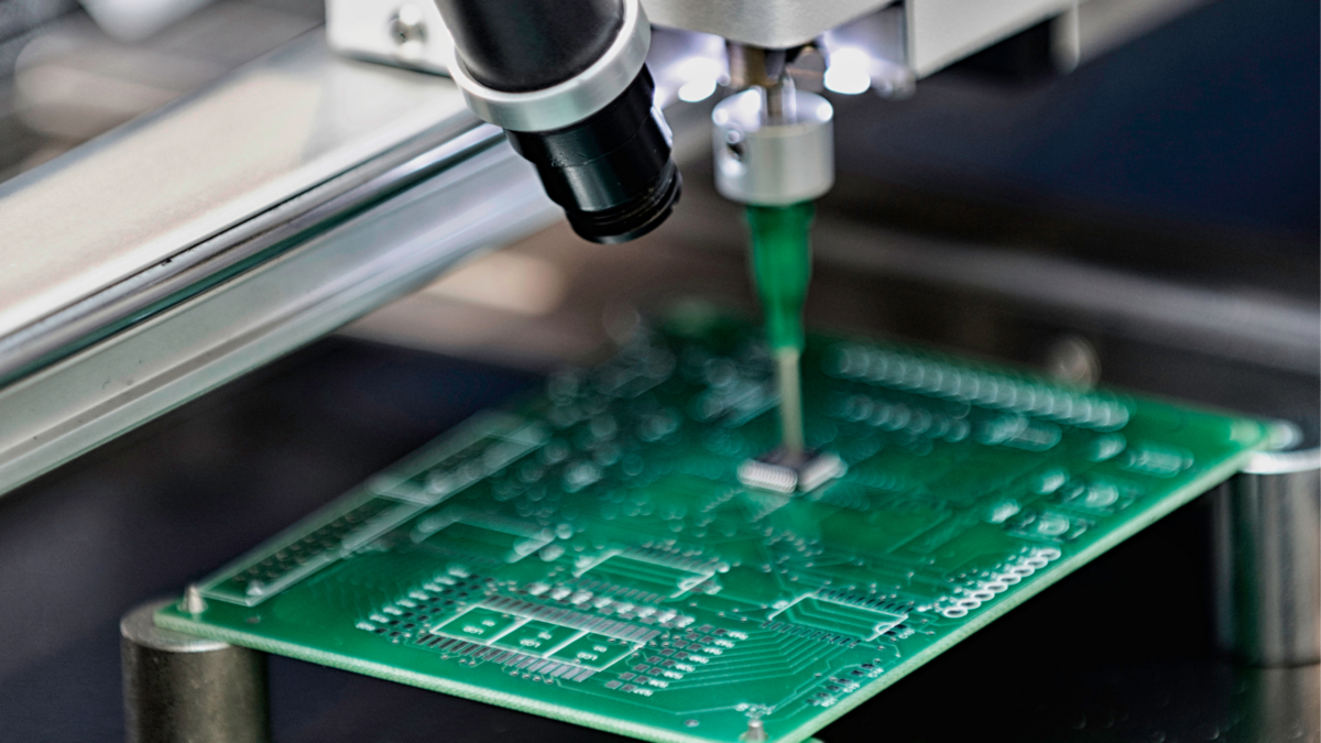
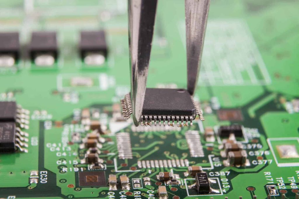
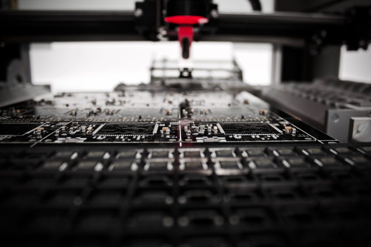
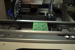
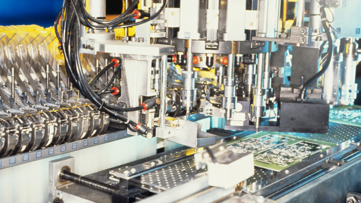
  • Automatically placing components using precision equipment
  • Reflow soldering surface mount components
  • Inserting and soldering through-hole components
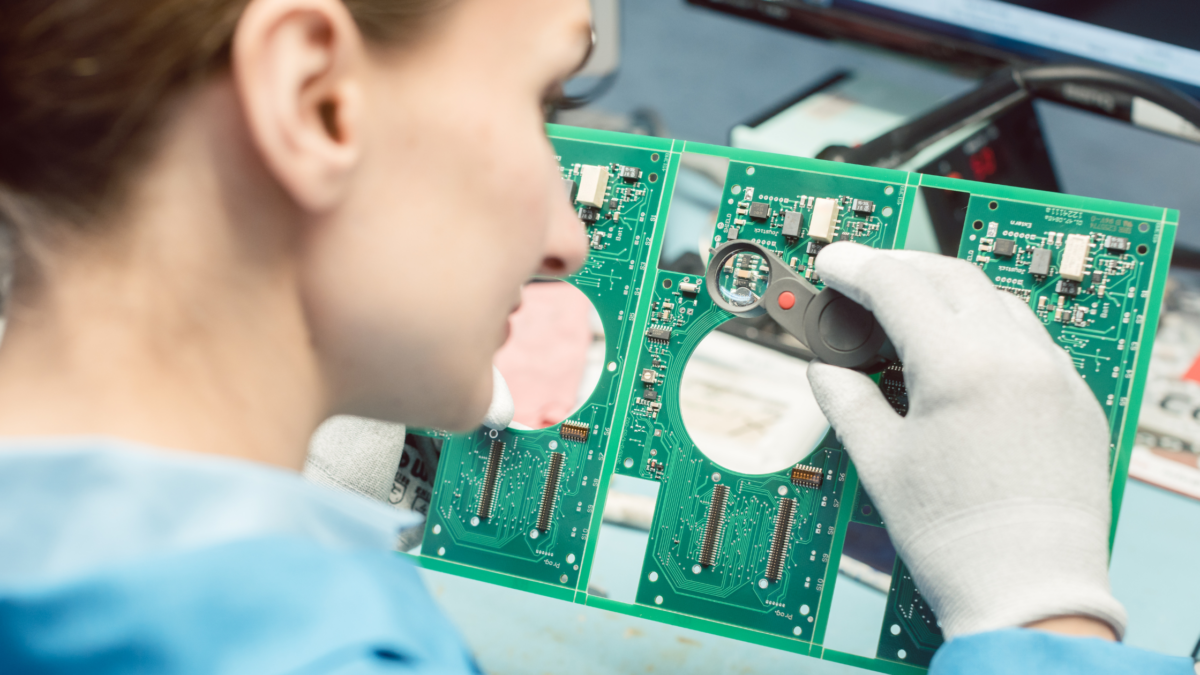
  • Inspecting completed assemblies for placement and solder quality

Nova also supports prototype, turnkey, and consigned PCB assembly projects, giving customers flexibility depending on their production and sourcing requirements.

Why the Printed Process Still Matters

The biggest advantage of printed circuit board production is repeatability. Once a design is finalized, manufacturers can reproduce the same trace patterns, component locations, and electrical connections across multiple boards.

That consistency is especially important as electronics become smaller and more complex. Modern PCBs can contain dense circuitry and numerous components while occupying relatively little space.

From printed circuit board production through final assembly, each step contributes to overall product quality. At Nova Engineering, we support customers with professional PCB assembly from early prototypes through ongoing production, with a focus on quality, consistency, and dependable manufacturing support at every stage.
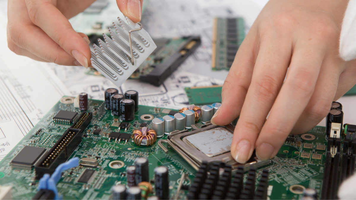
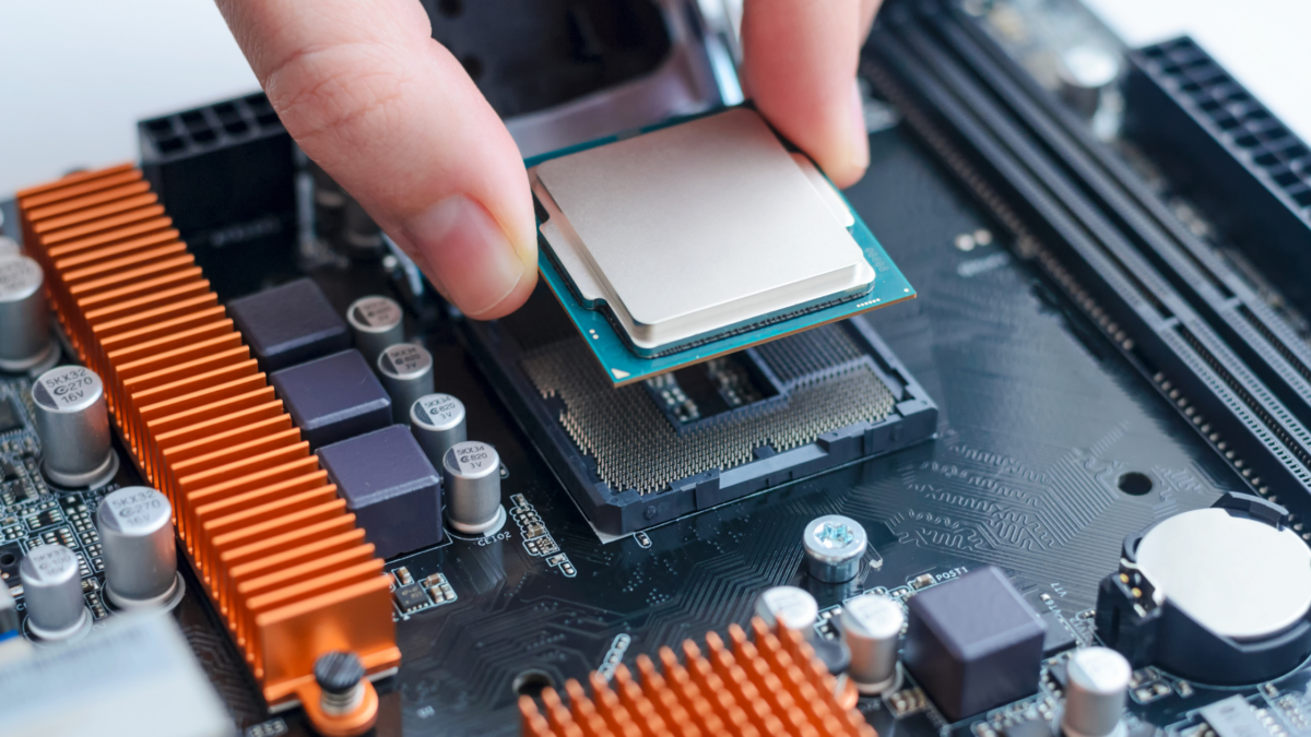
Printed Circuit Board Assembly (PCBA) Process- A Comprehensive Guide

Have you ever wondered about the structure of electrons that brings your electronic devices to life? Modern electronics have the printed circuit board assembly (PCBA) process that orchestrates this structure, transforming raw components into functional devices. Every electronic device we encounter is connected to the PCB in some way. Everything from smartphones, cars, home appliances, computers, etc., has these electronic building blocks.

Deepening technological advancements and evolving with time, the PCBA process transforms a design into a fully operational circuit. Although it may seem daunting at first, it is quite easy. Before that, you must know about the components used in PCBA.

The Basic Components Of PCB

The PCBA components are essential building blocks that transform a blank circuit board into a functional electronic device. Understanding these components is crucial for anyone delving into the intricate world of Printed Circuit Board Assembly (PCBA). When carefully orchestrated, these elements breathe life into the electronic devices that have become integral parts of our daily lives. Here we tell you about the key elements:

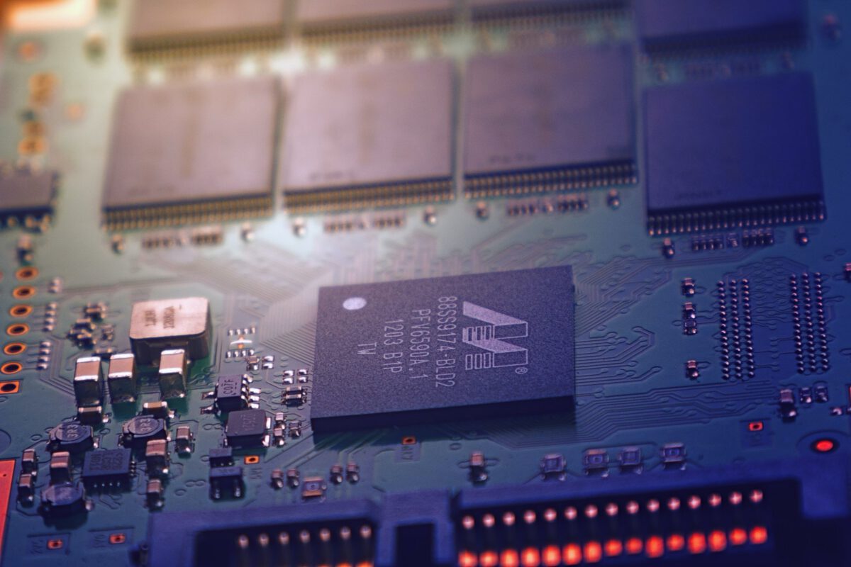
  • Integrated Circuits (ICs)
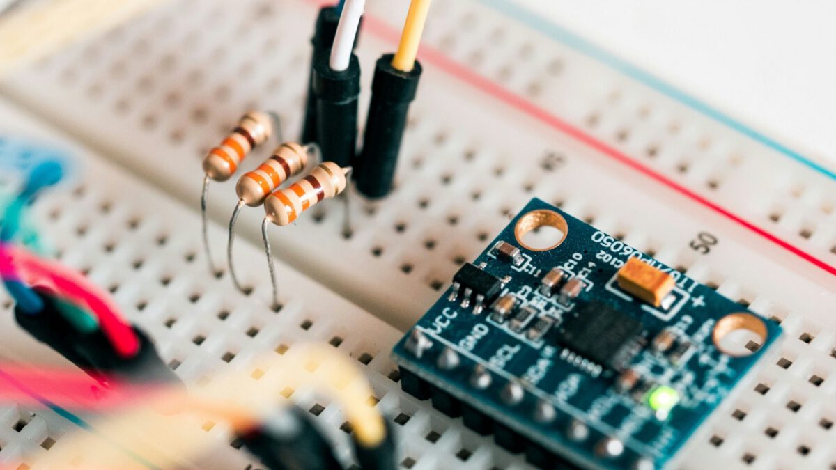
  • Resistors
  • Capacitors
  • Inductors
  • Diodes
  • Transistors
  • Connectors
  • Resonators and Oscillators
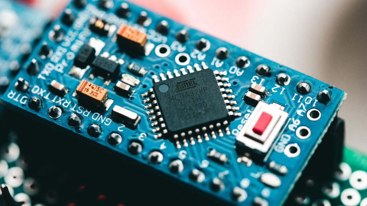
  • Microcontrollers
  • Sensors

The PCBA Process Steps

Step 1. Design and Layout

The Design and Layout phase of the Printed Circuit Board Assembly (PCBA) process is the foundational stage where the blueprint of the circuit board comes to life. Designers utilize specialized software, typically CAD (Computer-Aided Design), to meticulously plan the placement of components, signal traces, and layers. This step is pivotal in ensuring optimal functionality, as a well-thought-out design directly impacts the efficiency and manufacturability of the PCB. Designers must carefully consider factors like signal integrity, thermal management, and electromagnetic interference, laying the groundwork for the subsequent stages of the PCBA process.

Step 2: Fabrication of PCB

Fabricating a PCB involves transforming the design into a tangible board. This step includes selecting appropriate substrate materials, commonly fiberglass reinforced with epoxy and copper foils for the conductive layers. The fabrication process employs techniques like etching, layering, and coating to create the final PCB. The precision and quality of fabrication significantly influence the overall performance and reliability of the electronic device.

Step 3: Component Placement

Determining how components will be placed on the PCB is critical in the PCBA process. Engineers must choose between automated assembly machines or manual labor for precise component placement. This step’s precision is crucial as it directly affects the final electronic device’s functionality and efficiency. Careful consideration is given to optimizing the use of space on the PCB.

Step 4. Soldering

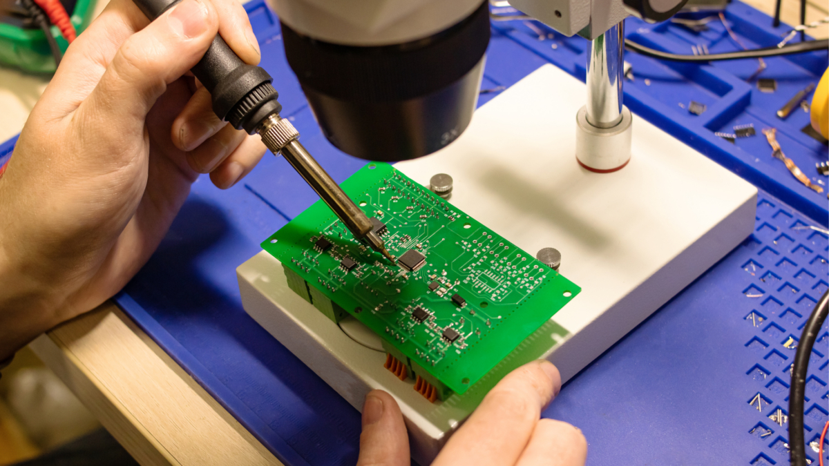
Soldering is the process that brings the PCB to life by creating electrical connections between components and the board itself. There are two primary techniques: Surface Mount Technology (SMT), where components are mounted directly onto the PCB surface, and Through-Hole Technology (THT), where components are inserted into drilled holes on the PCB. Reflow soldering, a common method, involves melting solder to form secure connections. The success of the soldering step ensures the reliability of the entire PCBA.

Step 5: Inspection and Testing

After assembly, thorough inspection and testing are crucial to guarantee the quality and functionality of the PCB. Visual inspection, automated optical inspection (AOI), and X-ray testing are common quality control measures. Functional testing ensures that the assembled PCB meets performance specifications, identifying and rectifying any defects before the final product reaches the end-user.

Step 6: PCB Design Considerations

PCB Design Considerations encompass the principles and guidelines that govern the layout, trace routing, and component placement during the design phase. These considerations are essential for achieving optimal performance, signal integrity, and reliability in the final product. Factors influencing design include the type of electronic components, the intended application, and the overall goals of the electronic device.

Step 7: Fabrication of PCB

Fabricating a PCB involves transforming the design into a tangible board. This step includes selecting appropriate substrate materials, commonly fiberglass reinforced with epoxy and copper foils for the conductive layers. The fabrication process employs techniques like etching, layering, and coating to create the final PCB. The precision and quality of fabrication significantly influence the overall performance and reliability of the electronic device.

Step 8: Component Placement

Determining how components will be placed on the PCB is critical in the PCBA process. Engineers must choose between automated assembly machines or manual labor for precise component placement. The precision of this step is crucial as it directly affects the functionality and efficiency of the final electronic device. Careful consideration is given to optimizing the use of space on the PCB.

Step 9: Soldering Techniques

Soldering techniques are integral to the PCBA process, determining how components are securely connected to the PCB. Surface mount technology (SMT) involves mounting components directly onto the PCB surface, while through-hole technology (THT) involves inserting components into drilled holes on the PCB. Reflow soldering, a widely used technique, melts solder to form reliable connections, ensuring the electronic device’s durability and performance.

Step 10: Inspection and Testing

Inspection and Testing are critical steps to verify the quality and functionality of the assembled PCB. Various quality control measures are employed, including visual inspection, automated optical inspection (AOI), and X-ray testing. Functional testing ensures that the PCB meets specified performance criteria, identifying and rectifying any defects before the final product reaches the end-user.

The PCBA process is a multifaceted journey from design to a fully operational circuit. Each step plays a role in ensuring the final electronic device’s functionality, reliability, and performance. As technology advances, the PCBA process evolves, presenting new opportunities and challenges for electronic manufacturers.

The Benefits of Outsourcing Circuit Board Assembly

Companies constantly seek ways to optimize operations, reduce costs, and maintain high-quality standards. One strategy that has gained significant traction in recent years is outsourcing circuit board assembly. By partnering with a reliable contract manufacturer, businesses can unlock various benefits that contributing to their overall success. This article will explore the advantages of outsourcing circuit board assembly.

Cost Savings

Cost reduction is often the primary driver behind outsourcing circuit board assembly. Establishing an in-house assembly line requires substantial equipment, infrastructure, and labor investment. By outsourcing, companies can eliminate or significantly reduce these upfront expenses. Contract manufacturers have already made these investments and can leverage their economies of scale to offer competitive pricing.

Outsourcing also eliminates the need for continuous training and retraining of in-house staff. With rapid technological advancements in electronics manufacturing, maintaining a highly skilled workforce can be costly and time-consuming. Contract manufacturers, on the other hand, specialize in hiring and retaining qualified assembly personnel.

Focus on Core Competencies

When companies outsource circuit board assembly, they can redirect their internal resources, including engineering and design teams, to focus on their core competencies. This enables them to innovate and develop new products more efficiently. By entrusting assembly to experts, businesses can streamline their operations and reduce the time to market for new products.

Access to Advanced Technology and Expertise

Contract manufacturers are at the forefront of technology in the electronics industry. They invest in state-of-the-art equipment, software, and processes to ensure circuit board assembly’s highest quality and efficiency. When you outsource, you can access this advanced technology and expertise without needing heavy capital investments.

Contract manufacturers often have experience working across various industries, which can be invaluable when solving complex assembly challenges or meeting specific industry standards and regulations.

Scalability and Flexibility

Outsourcing circuit board assembly provides businesses with scalability and flexibility that is difficult to achieve in-house. Contract manufacturers can quickly adjust production volumes to meet fluctuating demand, reducing the risk of overcapacity during slow periods or bottlenecks during high-demand seasons.

This flexibility is especially advantageous for companies with seasonal or unpredictable demand patterns. Contract manufacturers can adapt to these fluctuations without significantly changing the client’s operations.

Risk Mitigation

Electronics manufacturing carries inherent risks, from component shortages to quality control issues. Companies can share some of these risks with their contract manufacturing partners by outsourcing assembly. Experienced contract manufacturers have established supply chain networks and can navigate component shortages more effectively.

Additionally, contract manufacturers are highly focused on quality control and have stringent processes in place to ensure the reliability of the assembled circuit boards. This can help mitigate the risk of defects and costly recalls, harming a company’s reputation and bottom line.

Time Efficiency

Time-to-market is a critical factor in the electronics industry. Outsourcing circuit board assembly can significantly reduce the time it takes to get a product from concept to market. Contract manufacturers can start production quickly, eliminating the need for lengthy setup times to build an in-house assembly line.

Moreover, contract manufacturers often have established relationships with suppliers, which can expedite the procurement of components and materials. This timely access to resources can be a decisive advantage, especially in industries characterized by rapid technological change.

Conclusion

Outsourcing circuit board assembly offers many benefits, including cost savings, increased focus on core competencies, access to advanced technology and expertise, scalability, risk mitigation, and time efficiency. These advantages can translate into a competitive edge in the dynamic electronics industry.

However, choosing a reputable and experienced contract manufacturer is essential to reap these benefits fully. When considering outsourcing, businesses should evaluate potential partners carefully, looking for a track record of quality, reliability, and a commitment to meeting their needs.

By leveraging the strengths of a trusted contract manufacturer, companies can reduce costs, improve efficiency, and enhance their ability to innovate and respond to market demands swiftly. In an industry driven by innovation and competition, outsourcing circuit board assembly can be a strategic move that propels businesses toward sustained success.

Troubleshooting Common Issues in Circuit Board Assembly

Printed Circuit Boards, also known as PCB, must be manufactured because they need to have been manufactured according to the specific needs of the individual designing them.

Extensive development and changes would need to be made according to the scope of the circuit board, which is determined according to the project’s purpose.

However, it is important to know that a PCB is prone to many errors that may occur during the assembly phase of the 

creation process, whether it is due to an incident during the construction of the board or some inconsistencies that may lead to a faulty circuit board.

A circuit board is prone to many faults, but the good news is that there are certain steps to troubleshoot that you can utilize to rectify some common issues during the assembly phase of the circuit board.

Let us discuss the steps in greater detail, highlighting the entire troubleshooting process as a step-by-step guide.


PCB Troubleshooting Steps


Step #1: Cleaning

when troubleshooting to fix a faulty PCB, the first step is to thoroughly clean the board using alcohol wipes, specifically the part that has been infected, after which you need to dry the alcohol remaining on the part of the board where you have performed cleaning.


Step #2: Remove the Infected Padding

After you have performed thorough cleaning using alcohol, you need to take off the current padding that has been damaged. It is advised to do this using an exacto knife to ensure the pad has been peeled off without causing damage to the circuitry.


Step #3: Dispose the Laminate

Although not always the case, depending on the fault, there have been instances that the laminate also gets damaged, in which case, peel the laminating off as well.


Step #4: Take off Soldering Mask

Soldering is necessary for performing repairs on the circuit board, and the solder mask prevents the soldering iron from working on the board, so it is advised to remove any solder mask on the board.


Step #5: Rub Alcohol on all Spots

Once you have removed the mask, perform cleaning on those spots using alcohol to ensure that the entire board has been properly cleaned.


Step #6: Prepare the Area for Conductor Replacement

Before performing the replacement of the conductor in question, it is important to perform work on the spot to prepare it for the replacement.


Step #7: Choose the correct Circuit Frame

After examining and selecting the right circuit frame compatible with your replacement, choose the right conductor and remove the selection carefully from the frame, preferably with a small knife, to avoid contact with other parts involved within the circuitry.


Step #8: Prepping the Conductor

Once the appropriate frame and conductor have been determined, use the solder to work on the spot where the new conductor will be placed facing the trace of the old one.

After that, create the epoxy, and it is strongly advised to prepare it in small amounts because epoxy lasts for no more than 45 minutes.

After preparing the epoxy, apply it to the PCB and place it in the open air to ensure that the mixture dries up as soon as possible.


Step #9: Solder the new Pad

After the epoxy has been efficiently placed and set, it is time to fit the new conductor onto the trace using special tape.


Step #10: Let it Dry

The pad is not guaranteed to be set in place right after you have fit it onto the PCB, so it is recommended to hold the new pad in place, preferably using clamps to ensure it does not move while it dries.


Conclusion

Many issues can occur within a PCB during its assembly, such as gaps between the plating or the solder mask not being made properly between the pads, leading to the PCB not producing the intended results.

However, following these steps are a great way to troubleshoot a faulty PCB during its assembly phase to fix most of the common issues that can occur with the circuit board.

What are the Types of PCB Assembly Processes?

Printed circuit boards are used in practically anything electronic, including toys for kids, cars, and machinery for industrial manufacture. PCBs are crucial to numerous applications and are made from fibreglass, epoxy, metal components, and a green solder mask.

The components are arranged on it to enable the PCB to perform as intended. The PCB’s functionality is what matters most. Even if a tiny SMT resistor is not installed correctly or a little track is removed from the PCB maker, the PCB may still not function. Therefore, the parts must be put together correctly. When components are assembled, the PCB is referred to as an “assembled PCB” or “PCBA.” Here are some types of PCB Assembly processes:

Rigid-Flex Printed Circuit Board Assembly

Printed circuit boards, known as rigid-flex boards, combine stiff and flexible board technology. Depending on the application’s architecture, most rigid-flex boards are built from many layers of flexible circuit substrates outwardly or internally connected to one or more rigid boards. The flexible substrates are frequently moulded into the flexed curve during production or installation since they are intended to be flexible at all times.

Mixed Assembly

You cannot assemble various components using SMT technology, although it has replaced other mounting techniques in PCB fabrication. Then, the same board must be used for THT and SMT assembly. A mixed assembly uses various techniques but doesn’t require solder paste in the manufacturing process. Many components need to get welded with a surface mount arrangement on the board, except a few speciality components that are not accessible through the SMT process and must be constructed using mixed PCB.

Through-Hole Assembly

Electronic circuits are constructed utilising the through-hole assembly technique, in which leads are employed to position the components. It describes the assembly procedure, in which the leads are inserted into the pre-drilled holes before the components are joined to the board using either wave soldering or manual soldering. PCB design has historically used multi-layer, double-layer, and single-sided boards. Through-hole assembly is challenging to adapt to the needs of contemporary electronics.

Today, SMT technology has largely taken the place of through-hole assembly in the production of PCBs. However, some applications, such as those utilising electrolytic capacitors, connections, and substantial transformers, still call for through-hole installation.

BGA Assembly

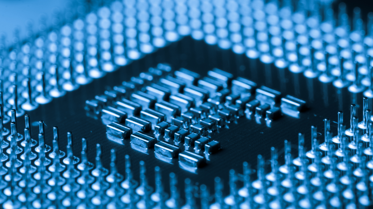
Surface-mount devices called ball grid arrays (BGA), also called chip carriers, are used for packaging integrated circuits. Microprocessors are installed permanently via BGA packaging. A BGA can accommodate more connector pins than a dual in-line or flat design. Instead of merely using the edge, the device’s entire bottom surface can be used. A perimeter-only type frequently has shorter traces than another, which improves performance at high speeds. These traces connect the package’s leads to the balls or wire and connect the package and the die.

SMT Assembly

Surface Mount Technology, or SMT, is the official name. SMT is a technique for attaching parts or components to circuit boards. SMT’s superior results and enhanced effectiveness have compelled the replacement of traditional PCB assembly methods. In the past, through-hole assembly was mostly used by PCB manufacturers to add components. However, welding technology has replaced the previous assembling technique in SMT.

All electronic businesses, including those in computers, phones, smartphones, home appliances, etc., employ PCBs made using the SMT assembly technique. Printing solder paste, mounting components, reflow soldering, and carrying out AOI or AXI are the basic procedures in SMT assembly.

Conclusion on Types of PCB Assembly Processes

Most PCBs that deliver high voltage or current have a separate plane for ground connections. The top layer’s electronic components are “Vias” connecting to the inner GND plane or signals layer. You can use any of the above processes, but ensure to have the right equipment.

Materials Selection for High Reliability PCB Assembly

The heart of any electronic device lies within its printed circuit board (PCB). Whether it’s a medical device, aerospace equipment, or automotive electronics, high reliability PCB assembly is essential. Achieving this level of reliability starts with careful materials selection. This article delves into the critical factors influencing material choice for high reliability PCB assembly.

Understanding the Application

Before diving into materials selection, it’s crucial to understand the application where the PCB will be deployed deeply. Different industries and use cases have unique demands, and the chosen materials should align with these requirements.

For example, aerospace and defense applications demand materials that can withstand extreme temperatures, high levels of radiation, and long-term exposure to harsh environments. Medical devices, on the other hand, require materials that meet stringent biocompatibility and sterilization standards. Automotive electronics must endure temperature fluctuations and vibration while maintaining long-term reliability.

Thermal Considerations

One of the primary factors in materials selection is the PCB’s ability to manage heat. Thermal performance is critical, especially in high-power applications where components generate substantial heat. The choice of materials, such as the substrate and copper thickness, directly impacts the PCB’s thermal conductivity and dissipation capabilities.

With their excellent thermal conductivity, materials like aluminum-backed PCBs are preferred in high-power LED applications. Similarly, materials with good thermal performance in automotive electronics help ensure the PCB can handle the heat generated by power electronics and maintain consistent functionality.

Dielectric Properties

Dielectric properties are vital for PCBs as they determine the material’s insulating ability and prevent electrical leakage. Materials with a high dielectric constant (εr) are suitable for applications where signal integrity is crucial, such as high-frequency RF circuits. Conversely, low-loss dielectric materials are essential for minimizing signal attenuation.

Careful selection of dielectric materials ensures that the PCB can maintain signal integrity and minimize losses in high-frequency or high-speed digital applications, whether it’s in telecommunications, satellite systems, or data centers.

Mechanical Durability

High reliability PCB assembly often requires materials that can withstand mechanical stress and vibration without compromising electrical performance. In automotive electronics, for example, the PCB must endure the rigors of the road without experiencing solder joint failures or component disconnections.

Materials with a high glass transition temperature (Tg) are more mechanically robust and better suited for applications where the PCB may be subject to extreme temperature variations. Reinforced materials, such as those with fiberglass or aramid reinforcement, can enhance a PCB’s mechanical durability.

Environmental Considerations

Environmental factors play a significant role in materials selection. Depending on the application, PCBs may be exposed to moisture, chemicals, and other harsh substances. Materials must be chosen to resist these environmental challenges.

For example, in medical devices that require sterilization, the PCB must be made from materials that can withstand repeated exposure to autoclaving or chemical sterilization processes. Similarly, automotive electronics must resist corrosion and moisture ingress, which can lead to premature failure.

Compliance and Certification

High reliability PCB assembly applications often require compliance with industry-specific standards and certifications. In particular, the aerospace, medical, and automotive industries have stringent requirements. Materials used in PCB assembly must meet these standards to ensure safety and reliability.

For example, the aerospace industry often requires compliance with standards like AS9100, while medical devices may need materials that meet ISO 10993 biocompatibility standards. Automotive electronics must adhere to automotive standards like AEC-Q100.

Cost Considerations

While high reliability PCB assembly is paramount, cost considerations are also relevant. It’s essential to strike a balance between materials that meet the performance and reliability requirements of the application while remaining within budget constraints.

Some materials, such as high-temperature FR-4, balance performance and cost well and are suitable for various applications. However, in cases where extreme reliability is needed, investing in more advanced materials may be justified.

Conclusion

The selection of materials for high reliability PCB assembly is a critical decision that directly impacts electronic devices’ performance, durability, and reliability. Each application has unique demands, and understanding these requirements is essential for making informed material choices.

By considering factors such as thermal performance, dielectric properties, mechanical durability, environmental resistance, compliance with industry standards, and cost, manufacturers can select the right materials to ensure their PCBs meet the highest reliability standards. In high-stakes industries like aerospace, medical, and automotive, where safety and performance are paramount, suitable materials can make all the difference in the success of a product.

The Future of Circuit Board Assembly: Trends and Innovations

Since it started, circuit board assembly has come a long way. With new tools and ideas, the future of circuit board assembly is enjoyable. In this blog, we will talk about the newest trends and innovations in circuit board assembly, as well as how they will affect the future of the business.

Industry Trends in Circuit Board Assembly

Various factors are impacting the assembly of circuit boards, including:

1. Miniaturization

Circuit board assembly is moving toward downsizing because people want smaller, more compact electronics. Manufacturers use new technologies and design methods to make smaller boards with all the needed parts and functions.

2. Surface Mount Technology

Surface mount technology (SMT) is becoming increasingly famous in circuit board assembly because it can use smaller parts and fit more on the same board. SMT makes it possible to place parts more precisely, which can improve the total performance of a device.

3. Automation

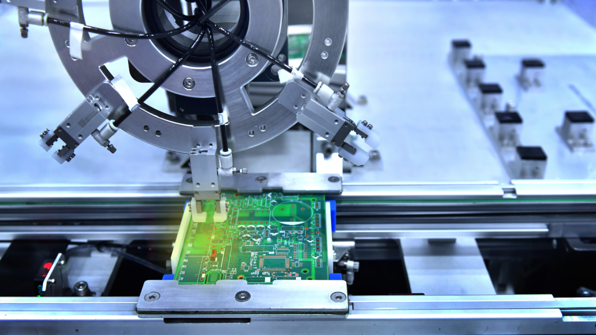
More and more makers use robots and automatic production lines to improve speed and reduce mistakes when assembling circuit boards. Automation also lets makers make boards with many components and smaller spacing between them.

4. Increased Use of Multi-layer Boards

Multi-layer boards are better than single-layer boards in several ways, such as having more circuits, being smaller, and having better signal integrity. As people want smaller and more complicated electronics, multi-layer boards are increasingly handy in circuit board assembly.

5. Use of Advanced Materials

A lot of circuit boards with new materials like high-temperature laminates and ceramic surfaces are entering the market. These materials have better temperatures and mechanical qualities, which makes it possible to pack more components into a gadget and make it work better.

Emerging Innovations in Circuit Board Assembly

Several emerging innovations are poised to transform the future of circuit board assembly, including:

1. Additive Manufacturing

Additive manufacturing, called “3D printing,” is a new way to make circuit boards. Additive manufacturing makes making complicated circuits and boards with unique forms possible. This process lets more personalized and new electronic products.

2. Flexible Electronics

Flex circuits, also known as flexible electronics, use bendable materials such as plastic or polyimide. This inception allows for circuit boards that can easily change shape and bend. This technology has several benefits, such as making boards last longer, making boards smaller, and making the design more flexible.

3. Internet of Things (IoT)

It is a network of gadgets that can share information and talk to each other. As IoT devices become more common, circuit board assembly must meet their specific needs, such as low power use, wireless connections, and small size.

4. Advanced Testing and Inspection Technologies

Circuit board assembly is increasingly likely to use advanced testing and inspection technologies, such as X-ray and automatic optical inspection. These technologies help makers find flaws and mistakes early on in the making process. This addition means that bad parts become less trash.

5. Artificial Intelligence (AI)

The emerging Artificial Intelligence (AI) technology can revolutionize circuit board assembly. By analyzing data from factory processes, AI programs can identify opportunities for enhancing efficiency and reducing errors.

The Future of Circuit Board Assembly

The latest cutting-edge technologies are altering circuit board assembly, making the future attractive. To be competitive and satisfy customers, manufacturers must adapt. Future circuit board assembly scenarios:

1. Increased Customization

3D printing and flexible electronics will allow manufacturers to make more personalized electrical devices for particular applications and use cases. Circuit board assembly must be more versatile in design and manufacture to accommodate diverse forms, sizes, and materials.

2. Improved Efficiency and Productivity

Automation and AI will continue to boost circuit board assembly efficiency and output, cutting human labor. Advanced testing and inspection technology will eliminate defective components, reducing reworks and discarded materials.

3. Greater Integration with IoT

IoT devices’ low power consumption and wireless connection will need circuit board assembly to merge smoothly with them. Manufacturers must implement IoT-compatible technology and procedures.

4. Continued Emphasis on Sustainability

Sustainable electronics will be in demand as customers grow more eco-conscious. Circuit board assembly must use sustainable materials and procedures to decrease electronic device waste and carbon impact.

5. Increased Collaboration and Integration

New technology and procedures will make circuit board assembly more integrated and collaborative. 3D printing involves understanding circuit board design and 3D printing technology, fostering cross-disciplinary cooperation.

Conclusion

Emerging technologies are altering circuit board assembly, making the future enjoyable. Manufacturers must embrace new processes and technology to stay competitive and fulfill customer needs. Future circuit board assembly possibilities include increasing customization, efficiency, productivity, IoT integration, sustainability, and cooperation. Manufacturers may build new, high-quality electrical gadgets that fulfill customer wants and progress the industry by keeping ahead of trends and embracing emerging technology.

The Importance of Quality Control in Circuit Board Assembly

In creating functioning electronic devices, the circuit board assembly process is crucial in manufacturing electronics. During this step, a technician or a machine solders the components onto the board. The assembly process is complex, and to guarantee the high quality of the result, meticulous attention is necessary to every little detail. This blog will investigate the significance of quality control in manufacturing since circuit board assembly includes quality control as an essential component.

What is Quality Control?

In the manufacturing industry, quality control is a procedure used to ensure that the final goods fulfill particular quality requirements. In assembling circuit boards, quality control entails examining each manufacturing process step, beginning with the original design and continuing through the final assembly, to verify that the end product satisfies the quality requirements.

The Importance of Quality Control in Circuit Board Assembly

Assembly of circuit boards requires stringent adherence to quality standards for the following reasons.

1. Ensures Product Reliability

When it comes to electrical equipment, dependability is essential. The device can create severe difficulties if it does not perform correctly. These problems include the loss of data or damage to equipment. The probability of a device failure is minimal when quality control ensures the circuit boards are correct and all components function appropriately.

2. Reduces Costs

The early identification of any problems by quality control helps reduce the rework or replacement of defective components somewhat later in production. This step helps save time and cut production costs, both of which contribute to improved profitability in the long run.

3. Improves Customer Satisfaction

The customer anticipates the product will be high quality, satisfy their requirements, and operate dependably. Controlling the quality of the completed product ensures that it lives up to these standards, increasing consumer happiness and loyalty.

4. Regulatory Compliance

When producing electronic equipment, manufacturers must adhere to several rules and standards. Examples are the Restriction of Hazardous Substances and the WEEE Directive. The completed product must be in line for compliance with these requirements. Failing to do so might result in both financial and legal repercussions.

5. Enhances Brand Reputation

Controlling quality contributes to developing a favorable brand reputation by showing that an organization is keeping its focus clear on manufacturing high-quality goods. This action may eventually result in more excellent sales and income due to increased trust and loyalty shown by the consumer base.

The Quality Control Process in Circuit Board Assembly

The quality control process in circuit board assembly involves several stages, including The quality control procedure for the construction of circuit boards consists of various steps including the following:

1. Incoming Inspection

When a component or material is ready to use at a production plant, it must first pass through a process known as “incoming inspection” to determine whether or not it satisfies the quality requirements. This step helps discover problems before the manufacturing process starts, reducing the risk of problems occurring later in production.

2. In-Process Inspection

Inspection of the boards and components at different phases of the production process is “in-process inspection.” This inspection guarantees that the boards and components are proper and operating appropriately. This action helps discover any flaws early in the process, decreasing the requirement for rework or discarding complex components in the product.

3. Final Inspection

The completed product is rechecked to satisfy all the necessary quality requirements before release. This verification involves testing the gadget to confirm its functions and that all its components operate appropriately.

Conclusion

It’s essential to have quality control when assembling circuit boards to ensure that the final product meets the necessary quality standards. It helps to increase customer happiness, assure product dependability, minimize costs, comply with laws, and promote brand reputation. Manufacturers may guarantee that their goods satisfy the high-quality standards demanded by consumers and authorities by developing a solid quality control procedure, ultimately leading to more significant sales and profitability.

Top 5 Latest Equipment You Need for Assembling Your Boards

While making PCBAs is a fun task, learning how the brains of all electronics are created offers joy and a sense of accomplishment. Each step of the assembling process is carefully thought out to produce a board that works flawlessly. Additionally, as electronics become more sophisticated, PCB manufacturing equipment is increasing and becoming more fascinating than ever.

Solder Paste Printing Machine

Solder paste is applied to the board as the initial step in PCB assembly. Usually composed of tin, lead, and silver alloys, solder paste is a grey-coloured goo formed from a combination of very microscopic metal particles. Consider it as the glue holding your finished board together. Components wouldn’t adhere to your bare board without it.

The PCB is covered with a stencil before the paste is applied. A PCB stencil is a piece of stainless steel with tiny laser-cut holes that allows solder paste only to be applied to the SMD pads, which are the board parts where the component connections will eventually be located on the finished PCB.

Glue Dispensing Machine

The glue dispensing machine uses glue dots on the PCB before component insertion to hold the component bodies until the leads and contacts are connected. This is crucial for reflow soldering or double-sided wave to prevent component drop-off and wave soldering, where the force of the solder wave may remove bigger components.

Reflow Soldering Machine

The most used soldering method for PCB assembly is reflow soldering. The assembly is transported via a conveyor via a lengthy, enormous oven called the reflow soldering machine once the board has been fully populated with components. As the PCB boards move through several temperature-controlled zones, the solder paste melts and steadily hardens to make reliable electrical connections between the component pads and their corresponding components.

The circuit board is moved along a conveyor system through the equipment’s various temperature zones. The solder paste is dried, heated, melted, wetted, and chilled before the components are soldered to the printed circuit board. The main component of reflow soldering is using an external heat source to heat the solder, causing it to melt, flow, and re-infiltrate the circuit board.

Automated Optical Inspection (AOI)

The boards have now been assembled, and testing and inspection are next. Automatic visual inspection is more crucial than ever due to the rise in the complexity of PCB boards. Even though you can still try to use your naked eyes to discover errors, manual inspection is ineffective for mass production since workers quickly become worn out, and errors are more likely to be overlooked. Testing PCBAs is essential in PCBA manufacture to prevent expensive re-manufacturing costs and material waste. AOI systems identify issues early in the production cycle, allowing for the modification of methods or the correction of specific boards.

AOI systems can complete tests formerly done by humans but much more quickly and accurately by using optical technologies to detect errors. The AOI machine uses high-resolution cameras to capture the board’s surface and create an image for analysis.

Functional Validation Test (FVT)

Before shipment, completed PCBs must pass Functional Validation Testing (FVT), which is the last phase. We are no longer merely looking for physical flaws like solder bridges or tombstones. The board is instead loaded with software, and we are testing to see if it will function when utilised in whatever application our customers have in mind.

Conclusion

Likely, components won’t be manually soldered when many PCBs need to be created. Expert assembly companies steps in to assist with the fabrication of both the bare boards and the assembly of all the parts into the Printed Circuit Boards, or PCBs.

Best Practices for Designing Circuit Boards for Assembly

Designing circuit boards for assembly is a meticulous process that significantly impacts electronic devices’ efficiency, reliability, and cost-effectiveness. Whether you’re working on a simple consumer product or a complex industrial system, adhering to best practices in PCB (Printed Circuit Board) design is crucial. This article will explore some essential best practices for designing circuit boards for assembly.

Plan for Assembly Early in the Design Process

Designing for assembly begins at the conceptual stage. Before diving into the detailed design, consider how the PCB will be assembled and the choice of components. This early planning can prevent costly redesigns and ensure the assembly process is as efficient as possible.

Use Standardized Components

Whenever possible, opt for standardized components. Standard components are readily available, reducing lead times and costs. Non-standard or custom features may lead to delays and increased expenses.

Keep Component Placement Logical

Logical component placement can significantly ease the assembly process. Group related components together and arrange them to minimize trace lengths. This reduces the chances of errors during assembly and enhances signal integrity.

Minimize Component Density

While compact designs are often necessary, overcrowding a PCB with components can lead to manufacturing challenges. A crowded PCB may be more prone to defects, which can be challenging to troubleshoot and repair. Aim for a balance between compactness and manufacturability.

Pay Attention to Component Orientation

Ensure that components are placed with the correct orientation. Misoriented components can lead to assembly errors and damage the board during soldering. Mark components with polarity clearly and use polarized connectors when necessary.

Use Design for Manufacturability (DFM) Guidelines

Consult DFM guidelines provided by your PCB manufacturer. These guidelines often include recommendations for component spacing, solder pad sizes, and other critical design elements. Following DFM guidelines can improve manufacturing yield and reduce the risk of defects.

Optimize for SMT Assembly

Surface-mount technology (SMT) is the predominant assembly method in modern PCB manufacturing. Design your PCB with SMT in mind, choosing components suitable for this assembly method. Ensure that your design includes solder pads for SMT components.

Consider Rework and Repairability

While striving for a defect-free design is ideal, it’s essential to consider rework and repairability. Components can fail or require replacement during the product’s lifecycle. Ensure that components can be desoldered and replaced without damaging the board.

Use High-Quality Footprints and Symbols

Accurate and high-quality footprints and symbols in your PCB design software are crucial. Errors in component footprints can lead to misalignment and assembly problems. Double-check the accuracy of all library components.

Minimize Noise and EMI

Pay attention to noise and electromagnetic interference (EMI) concerns. Proper grounding and shielding techniques can minimize noise and ensure the final product meets electromagnetic compatibility (EMC) standards.

Label and Document Thoroughly

Clear labeling and comprehensive documentation are essential for assembly and troubleshooting. Ensure that each component is labeled with its reference designator, and document any special assembly instructions, such as specific soldering temperatures or techniques.

Perform Design for Test (DFT)

Consider test design (DFT) principles when designing your PCB. Include test points or access points for in-circuit testing and functional testing. A PCB designed with testing in mind can help identify manufacturing defects early in the process.

Conduct Design Reviews

Regular design reviews with your assembly team, including PCB designers, engineers, and manufacturing personnel, can help identify and address potential issues before they become costly problems during assembly.

Prototype and Test Early

Prototyping and testing are invaluable steps in the design process. Building a prototype allows you to identify and rectify any assembly or performance issues before mass production begins.

Work with Experienced Manufacturers

Finally, collaborate with experienced PCB manufacturers and assembly partners. They can provide valuable insights and guidance throughout the design process, ensuring that your PCB design aligns with best practices for assembly.

Conclusion

Designing circuit boards for assembly requires careful planning and attention to detail. Following best practices throughout the design process can lead to more efficient assembly, higher manufacturing yields, and a more reliable electronic product. By considering assembly from the initial design stages and collaborating with experienced manufacturing partners, you can optimize your PCB design for assembly success.

RoHS Compliance and Lead-Free Soldering Techniques

One of the significant steps towards achieving environmental responsibility was the introduction of RoHS compliance regulations. RoHS, which stands for Restriction of Hazardous Substances, is a directive aimed at reducing the use of hazardous materials in electrical and electronic equipment. This directive has driven the adoption of lead-free soldering techniques in electronics manufacturing. In this article, we will explore RoHS compliance, its significance, and the lead-free soldering methods that have become central to it.

RoHS Compliance: A Brief Overview

The RoHS directive, formally known as Directive 2011/65/EU, originated in the European Union but has had a global impact on the electronics industry. Its primary objective is to restrict the use of specific hazardous substances in electronic and electrical equipment. These substances include:

  • Lead (Pb)
  • Mercury (Hg)
  • Cadmium (Cd)
  • Polybrominated biphenyls (PBB)
  • Hexavalent chromium (Cr6+)
  • Polybrominated diphenyl ethers (PBDE)

The RoHS directive applies to a wide range of electronic products, from household appliances to industrial machinery. Manufacturers and suppliers must comply with RoHS regulations to market their products in the EU and other regions that have adopted similar standards.

The Significance of RoHS Compliance

RoHS compliance carries several significant advantages and benefits, both for the environment and for consumers:

  • Environmental Impact

By restricting hazardous substances, RoHS helps reduce the environmental footprint of electronics manufacturing. It limits the release of toxic materials into the environment, thereby mitigating potential harm to ecosystems and human health.

  • Product Safety

RoHS compliance ensures that electronic products are safer for consumers. It reduces the risk of exposure to hazardous substances, particularly in consumer electronics and appliances that may come into direct contact with people.

  • Recycling and Disposal

RoHS-compliant products are easier to recycle and dispose of responsibly. They contain fewer hazardous materials, making them safer for recycling and preventing the contamination of landfills.

  • Global Market Access

Compliance with RoHS regulations enables manufacturers to access global markets. Many countries and regions outside the EU have adopted similar standards, making RoHS compliance essential for international trade.

Lead-Free Soldering Techniques

One of the most significant changes driven by RoHS compliance is the shift from lead-based solder to lead-free solder in electronics manufacturing. Lead-free soldering techniques have become central to achieving RoHS compliance. Here are key aspects of lead-free soldering:

1. Composition

Lead-free solder alloys are typically composed of various metals, with tin (Sn) being the primary component. Common alloys include Sn-Ag-Cu (SAC), Sn-Cu, and Sn-Ag. These alloys offer comparable or even superior mechanical and electrical properties to traditional lead-based solder.

2. Soldering Temperature

Lead-free soldering often requires higher temperatures than lead-based soldering. This can necessitate adjustments in soldering equipment, such as reflow ovens and soldering irons, to accommodate the higher melting points of lead-free alloys.

3. Compatibility

When transitioning to lead-free soldering, it’s essential to ensure that all components and materials used in the assembly process are compatible with lead-free solder. Some components may require adjustments or alternative materials.

4. Solder Paste and Flux

Lead-free solder paste and flux materials are formulated to work with lead-free solder alloys. These materials play a crucial role in ensuring proper wetting and bonding during the soldering process.

5. Process Control

Control over the soldering process is vital to achieve consistent and reliable solder joints. Manufacturers must fine-tune their soldering profiles to account for the characteristics of lead-free solder, ensuring proper reflow and minimizing defects.

Benefits of Lead-Free Soldering

The adoption of lead-free soldering techniques offers several benefits beyond RoHS compliance:

  • Environmental Responsibility

Lead-free solder reduces the environmental impact of electronics manufacturing by eliminating a highly toxic substance.

  • Health and Safety

Lead-free solder is safer for both manufacturing personnel and end-users, reducing the risk of lead exposure.

  • Recycling

Lead-free solder makes recycling and disposal of electronic products more environmentally friendly.

  • Global Market Access

Lead-free soldering techniques enable manufacturers to access global markets, ensuring their products comply with various environmental regulations.

  • Mechanical Strength

Lead-free solder alloys often exhibit improved mechanical strength, enhancing the reliability of soldered joints.

Conclusion

RoHS compliance and the adoption of lead-free soldering techniques have transformed the electronics manufacturing industry, promoting environmental responsibility, product safety, and global market access. While the transition to lead-free soldering presents challenges, the long-term benefits in terms of sustainability and safety make it a crucial step towards a more responsible and sustainable electronics industry. As technology continues to advance, ongoing research and development will further enhance lead-free soldering techniques, making them even more efficient and eco-friendly.

A Beginner’s Guide to Circuit Board Assembly

You may not realize it, but printed circuit boards are more important and common than you think. Present within a vast majority of the electronic devices we use daily, these circuit boards are a vital component that ensures the proper functionality of electronics.

Keeping this in mind, it is essential to understand that the assembly of these circuit boards is vital, primarily because they are a major component within electronics.

Because of the components and circuitry involved within an average PCB, the manufacturing process is incredibly complex.

Not only that, but the board you are working on also needs to be reliable enough to support the assembly process so that the resulting PCB does not turn out to be faulty.

Let us discuss this in further detail, exploring deeper into the concept of PCB assembly, understanding the resources needed, and the assembly process itself.

PCB Assembly: In Depth

Before going into the specifics of the overall process, let us first establish a foundation: the assembly process, taking a broader look at this part of PCB development.

Simply speaking, the initial state of a circuit board that has yet to go through any component installation is a printed circuit board, also known as the PCB.

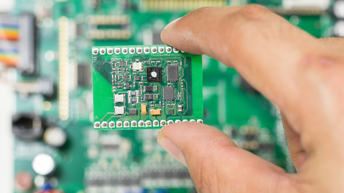
When the necessary electrical components have been installed onto the board, the resulting circuit board that we end up with is called the printed circuit board assembly, otherwise known as a PCBA.

Many people consider the PCB assembly and manufacturing process as the same thing, but that is not the case.

The main reason why assembling the circuit board is different is that when the PCB is being manufactured, it goes through a selection of different catering to the design and creation of the board.

However, assembly is what comes after the board has been developed after going through the design phase, involving the assembly of the electronic parts according to the main function of the PCB.

Resources Needed for PCB Assembly

Some certain tools and components are required to ensure that the overall assembling of the PCOB goes smoothly, and these include:

  • The printed circuit board itself
  • Transistors and other basic electronic components
  • A soldering flux
  • Necessary tools to perform a solder, including a soldering wire, soldering iron, and testing equipment.

Different Techniques of PCB Assembly

Even though the through-hole insertion technique for applying electrical components was the only way to develop PCBs, technological advancements have led to other methods, such as assembling a circuit board through SMT.

Assembling Using Thru-Hole Components

This type of PCB assembly involves certain components with wiring coming out of them, which go through the tiny holes within the PCB and are soldered.

When assembling a PCB using thru-hole components, it goes through a process called wave soldering, which involves the being applied in the form of a solder bar, which is put in an incredibly hot bath. This high temperature makes the solder stay molten and creates a wave-like design.

Once the wave has been made, the electrical components are passed through the molten state to be fitted within their places.

The overall assembling and solder process for these components includes:

  • Insertion of the necessary electronics
  • Applying the solder flux
  • Preheating the solder bar
  • Creating the wave solder
  • Cleaning and inspecting the PCBA
  • Testing the final product

Assembly Using SMT

Also known as surface mounting technology, this assembly process involves special components that do not contain any leads and do not need to go through any holes to be soldered.

Using this technology, they are directly soldered onto the PCB and are highly compatible with automation, leading to machinery automating the entire assembly process.

Conclusion

Many factors need to be considered when assembling a printed circuit board. However, with the right tools and components, you will not face any problems if you follow the steps mentioned above to assemble a PCB.

Advancements in Materials – Explore Latest in PCB Substrates

While traditional materials have served as the backbone of PCBs, a closer examination reveals inherent limitations and challenges. Understanding these constraints sets the stage for exploring cutting-edge solutions. The heart of innovation lies in printed circuit boards (PCBs) for the electronics industry. Within this dynamic industry, the substrates that underpin PCBs have emerged as a focal point of exploration and advancement. PCB substrates have moved from the foundations of traditional materials to the noncomposite wonders. By discussing how these advancements are reshaping industries and propelling us into an era of unprecedented electronic possibilities, we will know how to take leverage of this advancement.

What Are PCB Substrates?

Printed Circuit Board (PCB) substrates are the foundational materials that provide mechanical support and electrical insulation for the components on a PCB. These substrates serve as the base upon which the conductive paths and electronic components are mounted. Typically composed of insulating materials, PCB substrates play a crucial role in supporting the conductive traces that facilitate the flow of electrical signals throughout the circuit.

The choice of substrate material is vital, influencing the board’s performance, reliability, and overall functionality. Common materials used for PCB substrates include fiberglass-reinforced epoxy laminates (FR-4), which are widely employed in conventional PCBs, and more advanced materials like flexible polymers or ceramics for applications requiring flexibility or high-frequency performance.

Latest Innovations in PCB Substrates

PCB substrates provide a platform for the intricate interconnection of electronic components, enabling the creation of complex circuits that power a diverse array of electronic devices, from smartphones to industrial machinery. The continual innovation in PCB substrate materials contributes to the ongoing evolution of electronic technology, allowing for improvements in performance, miniaturization, and the development of new functionalities.

High-Frequency Materials

High-frequency materials represent a significant stride in the evolution of PCB substrates, particularly in response to the demands of new tech such as 5G communication. These materials exhibit low signal loss and enhanced signal integrity, crucial for transmitting data at higher frequencies. Common high-frequency substrate materials include polytetrafluoroethylene (PTFE) and ceramic-filled hydrocarbons. Adopting these materials enables the design of PCBs capable of supporting the rapid data rates required for next-generation wireless communication and other high-frequency applications.

Flexible and Rigid-Flex Substrates

The advent of flexible and rigid-flex substrates marks a departure from the rigid confines of traditional PCBs. Flexible substrates, often composed of polyimide, allow PCBs to bend or conform to non-planar surfaces, opening up new possibilities for wearable devices and unconventional form factors. Rigid-flex substrates combine flexible and rigid materials in a single board, balancing adaptability and structural integrity. This innovation is reshaping the design landscape, enabling the creation of foldable smartphones, flexible displays, and other compact electronic devices.

Nanocomposite Materials

Nanocomposite materials revolutionize PCB substrates by incorporating nanoparticles into the base material. These nanoparticles, often carbon-based, enhance mechanical strength, thermal conductivity, and electrical properties. The resulting PCBs exhibit improved performance, reduced size, and increased reliability. Nanocomposites are especially valuable in applications where size and weight are key factors, such as aerospace and medical devices. As technology advances, integrating nanocomposite materials into PCB substrates propels electronic devices into realms of previously unimaginable efficiency and capability.

Final Thoughts

Exploring the latest innovations in PCB substrates reveals a tapestry of technological breakthroughs poised to redefine electronic devices’ capabilities and design possibilities. The convergence of high-frequency precision, flexible adaptability, and microscopic enhancements of nanocomposite materials underscores the dynamic nature of electronic engineering. It sets the stage for a future where devices are interconnected and optimized for efficiency, performance, and versatility.

As we stand on the brink of this transformative era, the journey through these innovations in PCB substrates signals progress and a profound leap forward into the next generation of electronic design and functionality.

Common PCB Manufacturing Challenges and Their Solutions

The printed circuit board, PCB, bridges the gap between signals and powers. It makes sure power is directed within electronic devices. These fundamental components are often overlooked in sleek devices. Power is the backbone of connectivity and functionality. However, designing a PCB and making it fully functional can sometimes leave loopholes. These loopholes generate challenges that are caused during the manufacturing phase but show their failure during assembly.

The entire manufacturing of PCBs is riddled with challenges, including the delicate placement of minuscule components, the strategic management of heat, and the selection of materials resilient to diverse environmental factors. But with every challenge comes the solution, and if we fail to find it, we will jeopardize the performance and efficiency of electronic devices.

8 PCB Manufacturing Challenges And Solutions

While dissecting the routes of these challenges, we have curated a set of solutions from industry experts. Addressing these challenges isn’t just a matter of technical finesse; it is a strategic imperative. The smooth functionality of electronic devices hinges on successfully navigating these hurdles. Read on to learn more about the key challenges and the possible solutions.

Design For Manufacturability DFM

Design for Manufacturability (DFM) is a cornerstone for efficient PCB production. Ensuring that the design is conducive to manufacturing is vital in avoiding bottlenecks and errors. Challenges may arise when intricate designs pose component placement or thermal management difficulties. Solutions involve collaborative efforts between designers and manufacturers, incorporating DFM principles early in the design phase to optimize efficiency, reduce costs, and enhance overall manufacturability.

Solder Quality Control

The integrity of solder joints is paramount for the reliability of a PCB. Maintaining consistent solder quality can be challenging, leading to poor connections and premature component failure. Implementing rigorous quality control measures, including visual inspections and automated testing, is essential. Utilizing advanced soldering technologies and adhering to industry standards further ensures the production of PCBs with robust and reliable solder joints.

Slivers

Slivers, minute slivers of copper or other materials between traces, pose a challenge in PCB manufacturing, potentially causing short circuits or signal interference. Precision and thorough inspection are critical to identifying and eliminating slivers. Latest atest manufacturing methodsmethods , such as laser cutting and high-precision etching, help minimize the occurrence of slivers and ensure the integrity of the PCB design.

Missing Solder Masks

The absence of solder masks can result in bridging between solder joints, compromising the PCB’s functionality. Detecting and rectifying missing solder masks requires meticulous inspection and adherence to quality control protocols. Automated inspection systems and the careful application of solder masks during manufacturing are pivotal in preventing and addressing this challenge.

Acid Traps

Acid traps, where etching solutions can become trapped during manufacturing, threaten the
PCB’s integrity. This challenge can lead to uneven copper traces or other structural issues. Implementing effective rinsing and quality control processes in the manufacturing line helps mitigate acid traps, ensuring a clean and uniform etching process.

Material Defects

Material defects, such as inconsistencies in substrate materials, can compromise a PCB’s overall performance and reliability. Thorough material testing and quality assurance procedures are essential to identify and address these defects. Collaborating with reputable material suppliers and maintaining stringent quality control measures in the manufacturing facility are key strategies for minimizing material-related challenges.

BGA Spacing

Ball Grid Array (BGA) components present a specific challenge in PCB manufacturing due to their densely packed nature. Inadequate spacing can lead to issues during soldering and compromise the reliability of the connections. Precision in BGA component placement, utilizing advanced soldering techniques, and implementing thorough inspection processes are crucial for overcoming spacing challenges and ensuring the integrity of BGA connections.

Test Point Existence

Test points are essential for diagnosing and troubleshooting PCBs during and after manufacturing. The challenge is ensuring that these test points exist and are accessible. Incorporating standardized test point designs, strategically placing them on the PCB, and employing automated testing procedures contribute to overcoming this challenge, facilitating efficient testing and quality assurance throughout the manufacturing lifecycle.

Conclusion

There you go! By understanding the intricacies of PCB manufacturing challenges and proactively seeking solutions, manufacturers can ensure the reliability and quality of their products and position themselves at the forefront of technological advancement.

The Role of PCBs in IoT Devices: Challenges and Solutions

[et_pb_section fb_built=”1″ admin_label=”section” _builder_version=”4.16″ global_colors_info=”{}”][et_pb_row admin_label=”row” _builder_version=”4.16″ background_size=”initial” background_position=”top_left” background_repeat=”repeat” global_colors_info=”{}”][et_pb_column type=”4_4″ _builder_version=”4.16″ custom_padding=”|||” global_colors_info=”{}” custom_padding__hover=”|||”][et_pb_text admin_label=”Text” _builder_version=”4.24.2″ background_size=”initial” background_position=”top_left” background_repeat=”repeat” hover_enabled=”0″ global_colors_info=”{}” sticky_enabled=”0″]

For the IoT industry, PCBs are the unsung heroes who create functional connections in IoT devices. As the building block of electronic devices, PCBs play an important role in fostering IoT technologies’ efficiency, performance, and reliability. This thin board is made of insulating material with conductive copper track, allowing electronic components to route their connectivity for a circuit.

However, this building block comes with its own set of challenges that we will address so that you can see why your IoT device is acting up. Although these challenges can be a huge hindrance for us, they come with their solutions and an opportunity for us to learn and grow.

Challenges Faced by PCBs in IoT Devices

As IoT aims to connect and network devices, it is on OCB designs to mold how they work.

Size Constraints and Miniaturization

Printed circuit boards (PCBs) face a formidable challenge in IoT due to the devices’ ever-shrinking size requirements. As IoT applications demand increasingly compact and portable solutions, PCBs must grapple with the intricacies of miniaturization. This section explores the impact of size constraints on PCB design, examining the trade-offs between functionality and space efficiency. Strategies such as multi-layered PCBs and surface mount technology will be discussed to address the miniaturization challenge in IoT devices.

Power Consumption Issues

Efficient power management is critical in IoT devices where prolonged battery life and energy conservation are paramount. PCBs face the challenge of optimizing power distribution, minimizing energy loss, and ensuring overall energy efficiency. This segment delves into the intricacies of power consumption challenges, exploring how advanced power delivery systems, low-power components, and intelligent design can mitigate power constraints’ impact on PCBs in IoT applications.

Environmental Factors and Durability

IoT devices often operate in diverse and demanding environments, ranging from extreme temperatures to high humidity or corrosive conditions. PCBs must contend with maintaining functionality and structural integrity under such varied circumstances. This section explores the impact of environmental factors on PCB performance, delving into materials engineering, protective coatings, and design considerations that enhance the durability of PCBs in IoT devices.

Solutions to PCB Challenges in IoT Devices

With these solutions, it is prominent that IoT devices are revolutionizing PCBs’ basic structure and design.

Advanced Manufacturing Techniques

The implementation of advanced manufacturing techniques becomes crucial to address the challenges posed by size constraints and the need for miniaturization in PCBs for IoT devices. This section explores cutting-edge methods such as additive manufacturing, HDI (High-Density Interconnect) technology, and precision assembly processes. By adopting these approaches, engineers can optimize space utilization, enhance component integration, and overcome the limitations associated with the physical dimensions of IoT devices.

Energy-Efficient Design Strategies

Efficient power consumption is a cornerstone in the successful operation of IoT devices. PCBs play a pivotal role in achieving energy efficiency. This segment delves into design strategies that minimize power consumption without compromising performance. Topics include utilizing low-power components, smart power management systems, and implementing energy harvesting technologies. IoT devices can extend battery life and reduce their environmental impact by adopting these energy-efficient design principles.

Materials Innovation for Durability

PCBs must be robustly durable to ensure the longevity of IoT devices. This section explores innovative materials and coating technologies that enhance PCB resilience. A detailed examination of material science solutions will be provided, from corrosion-resistant materials to protective coatings that shield against harsh environmental conditions. By integrating these advancements, PCBs can withstand the rigors of varied environments, ensuring the reliability and durability of IoT devices.

As we delve into these solutions, it becomes evident that the evolution of PCB technology is intricately linked to overcoming the challenges posed by IoT requirements. Integrating advanced manufacturing techniques, energy-efficient designs, and innovative materials is paving the way for more resilient and high-performing PCBs in the rapidly expanding landscape of Internet of Things applications.

Wrapping Up

As we go through these challenges and their recurring solutions, we tend to address the designers’ perspective and also what IoT industries face. On the other hand, this era of innovation demands more user-friendly PCBs so that they can easily be integrated into the devices.

[/et_pb_text][/et_pb_column][/et_pb_row][/et_pb_section]

How Components on a Circuit Board Work Together to Power Modern Electronics

Have you ever thought about how much we rely on electronics every single day? From smartphones to industrial equipment, nearly everything we use depends on components on a circuit board working together seamlessly. Without these carefully designed systems, even the simplest device would not function.

At the core of modern electronics is the printed circuit board, often referred to as a PCB. It is not just a flat surface with parts attached. It is a precisely engineered platform where components interact to control power, process signals, and keep devices running efficiently. Understanding how these components work together helps highlight why quality PCB assembly matters, especially for companies like Nova Engineering that focus on reliability and precision.

Why Each Component Matters

Every PCB is designed with a purpose, and each element plays a specific role. When one piece fails, it can affect the performance of the entire system. That is why properly selected and assembled components on a circuit board are critical for long-term functionality.

Let’s break down some of the most important components and how they contribute to a working circuit.

Resistors: Controlling Electrical Flow

Resistors are one of the most common components on a circuit board. Their job is simple but essential. They regulate the flow of electrical current and help maintain safe voltage levels across the system.

Without resistors, circuits could easily overload, leading to overheating or permanent damage. They ensure that each part of the board receives the correct amount of power, which is especially important in sensitive electronics.

Capacitors: Storing and Releasing Energy

Capacitors act like temporary energy storage units. Among the key components, they store electrical energy and release it when needed.

They help stabilize voltage, filter noise, and support consistent performance. You will find capacitors in almost every electronic device, from consumer products to complex industrial systems.

Inductors: Managing Current and Magnetic Energy

Inductors are another type of passive component that plays a key role in managing electrical flow. These components on a circuit board store energy in a magnetic field when current passes through them.

They are commonly used in power supplies and filtering applications. Inductors help smooth out fluctuations in current and work closely with capacitors to maintain steady operation in circuits.

Transistors: Switching and Amplifying Signals

Transistors are among the most critical components on a circuit board because they act as both switches and amplifiers. They control the flow of electrical signals and allow circuits to perform complex tasks.

There are two primary types used in modern electronics:

  • Field Effect Transistors (FET)
  • Bipolar Junction Transistors (BJT)

These small but powerful components are essential for processing signals in everything from computers to communication devices.

Diodes: Directing Electrical Flow

Diodes ensure that electricity flows in only one direction. They protect circuits from damage caused by reverse current.

They are commonly used in power conversion, signal demodulation, and protection circuits. Without diodes, many electronic systems would be far less stable and reliable.

How It All Comes Together

While each part has its own role, the true power of a PCB comes from how all the components on a circuit board work together. Resistors regulate current, capacitors stabilize voltage, inductors manage energy flow, transistors process signals, and diodes control direction.

This level of coordination requires careful design and precise assembly. That is where experienced manufacturers like Nova Engineering make a difference. By ensuring that every component is correctly placed and properly integrated, they help create circuit boards that perform reliably in real-world applications.

The Bigger Picture for Modern Electronics

From everyday consumer devices to advanced industrial systems, the performance of electronics depends on the quality of the components on a circuit board and how well they are assembled. Even the smallest detail can impact overall functionality.

As technology continues to evolve, the demand for high-quality PCB assembly will only grow. Understanding how these components work together not only builds appreciation for modern electronics but also highlights the importance of choosing the right manufacturing partner.

PCB Troubleshooting: Common Assembly Issues and How to Catch Them Early

PCB troubleshooting is an important part of building reliable electronics. Even a well-designed board can run into assembly-related problems if materials, placement, soldering, or inspection steps are not carefully managed. In 2026, as boards continue to become smaller, denser, and more complex, it is less about guessing and more about following a consistent process that identifies issues early.

For manufacturers and product teams, the goal of pcb troubleshooting is not just to fix a bad board after the fact. It is to understand what caused the issue, prevent it from repeating, and keep production moving with confidence. That matters whether you are building a prototype, preparing for a new product introduction, or scaling into production.

Start With the Most Common Problem Areas

Many assembly issues can be traced back to a few core areas. Solder defects remain one of the most common reasons boards fail inspection or testing. These can include insufficient solder, solder bridges, cold joints, tombstoning, or poor wetting. Component placement problems are also common, especially on high-density boards where alignment tolerance is tight.

Another major area in pcb troubleshooting is materials verification. Incorrect parts, outdated components, polarity mistakes, and kit inconsistencies can all create avoidable failures. In some cases, the board itself is not the problem at all. The issue may come from the bill of materials, design file mismatch, or an error introduced before the board ever reached the line.

Use a Step-by-Step PCB Troubleshooting Process

Effective pcb troubleshooting works best when it follows a clear sequence instead of jumping straight to repair. A practical process often looks like this:

1. Review the documentation

Start by checking the Gerber files, BOM, assembly drawings, and revision level. Small file mismatches can create larger downstream issues.

2. Inspect the board visually

Look for missing parts, wrong orientation, solder bridges, lifted pads, or obvious handling damage.

3. Verify materials and placement

Confirm that the correct components were used and placed in the right locations.

4. Check solder quality

Review joints for consistency, coverage, and possible defects that could affect conductivity or reliability.

5. Run electrical or functional testing

If the board looks acceptable but still fails, test continuity, isolation, and real-world function to narrow down the issue.

6. Trace the root cause

Strong pcb troubleshooting does not stop at identifying the symptom. It asks why the defect happened and what process should change to prevent repeat failures.

Inspection Technology Matters More Than Ever

Modern pcb troubleshooting depends heavily on inspection systems and process control. Automated Optical Inspection, or AOI, is especially useful for catching placement and solder issues that may be easy to miss during manual review. Functional testing and final verification are also critical when boards are headed into demanding applications.

This is one reason manufacturers are placing more value on structured quality systems in 2026. As assemblies grow more compact and performance expectations rise, troubleshooting becomes faster and more reliable when it is backed by documented inspection procedures, trained staff, and repeatable workflows. Nova highlights automated SMT inspection, 100% final visual inspection, and in-house engineering support as part of its assembly process.

Why Prevention Is a Big Part 

The best pcb troubleshooting efforts begin before assembly starts. Design for Manufacturability review can uncover pad sizing issues, rotation problems, and other layout concerns that may create defects later in production. Material planning, kit verification, and inspection checkpoints also reduce the chance of rework and delays.

For companies moving from prototype to larger production volumes, this approach can make a major difference. Catching issues early helps reduce scrap, protect schedules, and improve long-term product reliability. That is especially important in industries where consistency matters, such as medical, aerospace, military, telecommunications, and industrial electronics.

Building Better Boards From the Start

It is not just about repairing defects. It is about creating a smarter assembly process that supports quality from the first build onward. When manufacturers combine careful documentation review, strong inspection methods, and root-cause analysis, they put themselves in a better position to deliver dependable boards with fewer surprises.

For teams that need support from prototype through production, working with an experienced assembly partner can make pcb troubleshooting more efficient and far less reactive. Nova Engineering’s focus on prototype, turnkey, consigned, and partially consigned PCB assembly reflects the kind of process-driven support that helps customers move forward with greater confidence.

Quality Control of Printed Circuit Boards in Modern Electronics

The quality control of printed circuit boards is one of the most critical factors in producing reliable, high-performing electronic devices. From consumer electronics to medical equipment and industrial systems, printed circuit boards (PCBs) serve as the foundation for functionality. As designs become more compact and complex in 2026 and beyond, manufacturers rely on rigorous quality control to ensure boards perform exactly as intended—every time.

This article explains what quality control of printed circuit boards involves, why it matters, and how modern inspection and testing methods help prevent failures before products ever reach the field.

What Is It?

Quality control of printed circuit boards refers to a structured set of inspections, tests, and verification steps used throughout the PCB manufacturing and assembly process. These checks ensure that materials, components, solder joints, and electrical connections meet defined performance and reliability standards.

Unlike basic visual checks used in the past, today’s quality control of printed circuit boards relies on automation, data tracking, and industry standards to catch defects early—before they turn into costly failures.

Why Quality Control Matters in PCB Manufacturing

The importance has grown significantly as electronics have become smaller, faster, and more interconnected. Even a minor defect—such as a solder bridge, missing component, or micro-crack—can lead to intermittent failures that are difficult to diagnose later.

Key reasons quality control is essential include:

Ensuring Long-Term Reliability

Devices are expected to operate consistently over long lifespans, often in harsh environments. Proper quality control of printed circuit boards helps confirm that electrical connections are sound and components function as designed under stress.

Reducing Manufacturing Costs

Identifying defects early reduces rework, scrap, and warranty claims. In 2026, manufacturers increasingly focus on “right-first-time” production, where strong quality control lowers total production costs.

Supporting Regulatory and Industry Compliance

Many PCBs must comply with standards such as IPC-A-610, RoHS, REACH, and ISO-based quality systems. Quality control of printed circuit boards ensures compliance and helps manufacturers avoid costly delays or penalties.

Protecting Brand Reputation

Consistently high-quality PCBs translate directly into reliable end products. This builds trust with customers and strengthens long-term brand credibility.

Key Stages: Quality Control of Printed Circuit Boards

Incoming Material Inspection

Before assembly begins, components and bare boards are inspected to verify authenticity, correct specifications, and physical condition. This step is increasingly important due to global supply chain variability and counterfeit risks.

In-Process Inspection

During assembly, boards are inspected at multiple stages to catch issues as they happen. Common in-process quality control methods include:

  • Automated Optical Inspection (AOI) to detect placement and solder defects

  • X-ray inspection for hidden joints such as BGAs and QFNs

  • Solder paste inspection (SPI) to ensure accurate paste deposition

These steps allow manufacturers to correct issues before they compound.

quality control of printed circuit boards- Nova

Electrical and Functional Testing

This also includes electrical testing to verify continuity, isolation, and signal integrity. Functional testing confirms that the assembled board performs as expected in real-world operating conditions.

Final Verification

Before shipment, boards undergo a final quality review to confirm they meet all design, performance, and documentation requirements. This ensures consistency across production runs.

Building Confidence Through Consistent Quality

Strong quality control of printed circuit boards is not just a manufacturing requirement—it’s a strategic advantage. When implemented correctly, it ensures product reliability, reduces long-term costs, and supports compliance in a demanding regulatory environment.

By investing in thorough inspection, testing, and process control, manufacturers can deliver printed circuit boards that perform reliably across applications and industries—meeting the expectations of both customers and the technologies they rely on. At Nova Engineering, this commitment to quality control is built into every stage of PCB assembly, helping ensure consistent performance from prototype through production.

When to Outsource Printed Circuit Board Assembly

Understanding when to outsource printed circuit board assembly is critical in today’s fast-paced electronics industry. As product designs become more complex and demand fluctuates, many companies are rethinking whether to keep PCB assembly in-house or partner with a trusted contract manufacturer.

Outsourcing isn’t just about reducing costs—it’s about aligning your capabilities with your strategic goals. Done right, it enables faster production, fewer quality issues, and a more agile response to changing market needs.

The High Cost of In-House Assembly

Building and maintaining an in-house assembly line requires substantial investment. From specialized equipment like pick-and-place machines and reflow ovens to ongoing technician training and quality assurance systems, the operational burden is high. This infrastructure also needs to evolve alongside rapid changes in PCB technology.

One of the clearest signs of when to outsource printed circuit board assembly is when these costs begin to outweigh the value of keeping production internal. Contract manufacturers like Nova Engineering have already made those investments—and they spread them across multiple clients, lowering the cost per unit. Outsourcing lets you tap into that infrastructure without having to build it yourself.

Indicators It’s Time to Consider Outsourcing

There’s no one-size-fits-all answer to when to outsource printed circuit board assembly, but several signs can indicate it’s time to shift to an external partner:

  • Increased lead times due to resource limitations or equipment bottlenecks 
  • Inconsistent quality or higher failure rates on delivered boards 
  • Delayed product launches from stretched internal teams 
  • Difficulty sourcing components or keeping up with inspection requirements 
  • Frequent demand fluctuations that strain production planning 

If any of these sound familiar, outsourcing can relieve pressure and improve output reliability.

Benefits of Contract Manufacturing Partnerships

Understanding when to outsource printed circuit board assembly is key to unlocking the advantages of a reliable contract manufacturing relationship. Partnering with a trusted PCB assembly provider opens the door to specialized capabilities that might not exist in-house. Contract manufacturers are constantly upgrading their tools, certifications, and knowledge to meet industry demands—from aerospace to medical and automotive applications.

When you outsource to an experienced manufacturer, you gain access to:

  • Advanced manufacturing techniques like fine-pitch BGA placement or HDI 
  • Cleanroom and ESD-controlled environments for sensitive electronics 
  • Dedicated quality control systems, including AOI, X-ray, and functional testing 
  • Knowledge of regulatory compliance, such as IPC-A-610, ISO 9001, and RoHS 

These advantages are especially valuable when you’re scaling up, launching a new product, or handling complex board designs that require consistent precision.

Preserving Internal Focus and Speed

One of the most overlooked benefits of outsourcing is that it lets your engineering and product teams stay focused. Knowing when to outsource printed circuit board assembly can help ensure internal resources aren’t tied up solving manufacturing issues, which often delays development timelines.

By outsourcing PCB assembly, you free up key personnel to do what they do best—designing, testing, and iterating on new innovations. This clearer focus can accelerate development cycles and reduce time to market—an increasingly valuable advantage in competitive product categories.

Building in Flexibility for Growth

As demand changes, so should your production strategy. Rigid in-house operations often struggle to keep pace with variable order sizes, evolving product specs, or sudden market shifts. Knowing when to outsource printed circuit board assembly helps you build flexibility into your business model.

Contract manufacturers can adapt quickly to changing volumes or requirements. Whether you’re producing hundreds or tens of thousands of boards, they offer scalable capacity without the need for internal investment or delays.

A Strategic Move Toward Smarter Manufacturing

Outsourcing printed circuit board assembly isn’t a shortcut—it’s a strategic choice that allows companies to grow more efficiently. Knowing when to outsource printed circuit board assembly matters most when your team is spread too thin, production costs are rising, or your technology is falling behind, and it’s time to evaluate your options.

A qualified contract manufacturer like Nova Engineering can help you lower risk, maintain high quality, and speed up delivery—while your team stays focused on innovation. For many companies, that’s the difference between staying competitive and falling behind.

6 Educational Circuit Board Facts That Power Modern Electronics

From the smartphone in your pocket to the industrial systems that run factories, circuit boards are at the heart of nearly all electronic technology. Yet most people know surprisingly little about what makes these boards work—or why they’re so important. Here are six essential circuit board facts that offer insight into the design, functionality, and innovation behind today’s printed circuit boards (PCBs).

1. Circuit Boards Simplify Complex Electrical Systems

One of the most important circuit board facts is that PCBs reduce the need for bulky wiring. Before PCBs, electronics were assembled using point-to-point wiring, which was not only messy but also prone to human error and difficult to replicate at scale. Printed circuit boards replaced this with pre-designed copper traces, streamlining the design, reducing manufacturing errors, and making mass production of electronics feasible.

PCBs serve as both the physical structure and the electrical connection platform for components such as resistors, capacitors, diodes, and microchips—all neatly arranged on a single board.

2. There Are Several Types of PCB Configurations

Another essential entry in circuit board facts: not all PCBs are the same. The type of circuit board used depends on the application’s complexity and requirements. Common types include:

  • Single-layer PCBs – Ideal for simple electronics like calculators and LED lights

  • Double-layer PCBs – Used in more advanced consumer electronics

  • Multilayer PCBs – Found in servers, industrial equipment, and advanced computing

  • Rigid-flex PCBs – Used in aerospace, medical, and compact consumer devices

Each type supports specific performance needs, cost levels, and design constraints.

3. PCBs Can Have Over 50 Layers

One of the more surprising facts is that advanced PCBs can consist of more than 50 layers of copper and insulating material. These multilayer boards are essential for devices that require high-speed data transmission, complex signal routing, or power distribution across multiple channels.

High-performance computers, 5G infrastructure, and aerospace systems rely on these densely packed boards to maintain reliability and speed without increasing the device size.

4. Surface Mount Technology Has Replaced Older Techniques

Decades ago, through-hole technology was the standard for mounting components on a PCB. Today, Surface Mount Technology (SMT) is the dominant method. SMT allows components to be mounted directly onto the surface of the board, enabling:

  • Smaller board sizes

  • Faster automated assembly

  • Higher component density

This evolution in assembly methods is one of the most important circuit board facts influencing modern electronics design.

5. Circuit Boards Are Designed Using Specialized Software

Designing a circuit board isn’t done by hand—it requires precision software tools. Engineers use computer-aided design (CAD) programs like Altium Designer, Eagle, or KiCad to lay out the copper traces, component placement, and via locations. These tools generate Gerber files, which are the standard file format used by manufacturers to fabricate PCBs.

This digital design-to-manufacturing workflow ensures every printed circuit board meets exact specifications and performance requirements.

6. Clean Manufacturing Matters More Than You Think

One of the lesser-known but critical circuit board facts is how important cleanliness is during manufacturing. Dust, oils, or static discharge can compromise conductivity or damage sensitive components. That’s why PCB manufacturing facilities often follow strict environmental controls, similar to cleanrooms used in semiconductor fabrication.

Maintaining a controlled environment ensures higher reliability, longer board life, and reduced failure rates—especially in high-stakes industries like medical, military, or aviation.

Why These Circuit Board Facts Matter

Understanding these circuit board facts helps demystify the technology that powers modern life. Whether you’re designing consumer electronics, industrial systems, or mission-critical devices, knowing how PCBs function—and how they’re evolving—helps you make smarter design, sourcing, and manufacturing decisions.

At Nova Engineering, we specialize in assembling reliable, high-performance circuit boards for a wide range of industries. From prototype to production, we ensure every layer, connection, and component is built with precision and care.

Why are Circuit Board Assemblies Printed?

Before modern advancements in electronics, connecting components in a circuit was a manual and error-prone task. Engineers relied on point-to-point wiring to create circuits inside radios, computers, and early appliances. This method was time-consuming, difficult to repair, and prone to short circuits. Everything changed when the concept of a circuit board printed with conductive paths emerged.

The shift to printed circuit boards (PCBs) revolutionized electronic design and manufacturing. Instead of hand-wiring every connection, engineers could now design a board with etched copper traces to automatically route electricity between components. This innovation drastically improved efficiency, reliability, and scalability.circuit board printed- nova engineering

The Origins of Printed Circuit Boards

In 1936, Austrian engineer Paul Eisler introduced the first concept of a circuit board printed with copper pathways. He created a non-conductive base material with a printed copper circuit on top, which allowed components to be soldered onto predefined traces. While early versions looked nothing like today’s compact multilayer PCBs, the foundational idea remains the same.

The transition to printed technology laid the groundwork for the mass production of electronic devices. It also reduced human error and allowed for more precise circuit design, which is essential in everything from consumer electronics to aerospace systems.

How Is a Circuit Board Printed Today?

Modern PCB technology begins with a simple sheet of copper laminated onto a fiberglass-reinforced epoxy material (commonly FR4). The steps to manufacture a printed circuit board are precise and controlled to ensure quality and consistency.

1. Design and Gerber Files

The first step in creating a circuit board printed design is using computer-aided design (CAD) software. Engineers generate what’s known as Gerber files—digital blueprints that detail the layout of copper traces, pads, vias, and holes. These files drive every phase of manufacturing.

2. Drilling

Once the layout is finalized, the board undergoes a drilling process to create holes that will later hold through-hole components or vias. Each circuit board printed design includes precision-placed holes, created by computer-guided drills based on the Gerber file.

After drilling, the board is cleaned to remove any dust or debris, ensuring proper adhesion of materials in later steps.

3. Creating Copper Traces (Etching)

To create the conductive pathways, a photosensitive resist layer is applied to the copper surface. A light is used to expose only the desired circuit pattern. After exposure, the unprotected copper is removed using a chemical etching process, leaving behind the intricate network of copper traces.

This etching step is what transforms a blank copper sheet into a PCB with a custom circuit layout.

4. Solder Mask and Silkscreen

Once the traces are etched, a green (or sometimes blue, red, or black) solder mask is applied. This layer insulates the copper traces and prevents solder bridges between components during assembly.

The silkscreen layer is printed next. It provides labels, part numbers, and component identifiers directly on the circuit board printed surface, guiding technicians during assembly.

The Value of Printed Circuit Board Assemblies

A PCB with accuracy enables faster assembly, more compact device designs, and easier mass production. Whether used in smartphones or spacecraft, printed circuit boards provide the foundation for electrical functionality and performance.

Printing circuit boards also enables automation in the next stage: PCB assembly. Using automated pick-and-place machines, manufacturers can quickly place thousands of components onto a circuit board with pinpoint accuracy. Combined with reflow soldering and inspection, this results in highly reliable electronic systems.

The Role of Printing in Modern PCB Manufacturing

Today, the term printed circuit board refers not only to the physical traces on a PCB but also to the broader manufacturing process that allows for miniaturization and performance in advanced electronics. As devices become smaller and more powerful, printed circuit board technology evolves alongside them.

From its origins in early radios to powering high-speed computers, the innovation of having a circuit board printed with precise paths has transformed electronics forever. For engineers and manufacturers, it remains one of the most essential building blocks of any electronic design.

Types of PCB Assembly Processes: An In-Depth Guide

Printed circuit boards (PCBs) are the core of nearly every modern electronic device—from smartphones and laptops to medical equipment and industrial systems. But behind every functioning PCB is a carefully executed series of PCB assembly processes that bring the board to life.

If you’re wondering what these processes are and how they differ, this guide will walk you through the most common types of PCB assembly processes and explain when and why each is used.

What Is PCB Assembly?

Before diving into the types of PCB assembly processes, it’s important to understand what PCB assembly entails. PCB assembly (also known as PCBA) refers to the process of attaching electronic components to a blank printed circuit board using soldering techniques.

Without a reliable assembly process, even a perfectly designed board will fail to function. That’s why selecting the right method is key to performance, cost, and reliability.

Surface Mount Technology (SMT) Assembly

Surface Mount Technology (SMT) is the most widely used of all PCB assembly processes. It involves placing components directly onto the surface of the PCB using solder paste and a reflow oven.

Why choose SMT?

  • Compact and efficient for high-density designs

  • Faster and more cost-effective for large runs

  • Widely used in consumer electronics, medical devices, and more

SMT allows for high-speed automated assembly and is ideal for miniaturized components.

Through-Hole Assembly

Through-hole assembly is a traditional method where component leads are inserted through pre-drilled holes in the PCB and soldered on the opposite side. Though it’s been largely replaced by SMT, through-hole is still useful for components that require strong mechanical bonds.

Best for:

  • Connectors, transformers, and large capacitors

  • Industrial and high-power applications

  • Environments with high mechanical stress

While slower and more manual, through-hole remains valuable for certain durable designs.

Mixed Technology Assembly

Mixed technology combines SMT and through-hole components on a single PCB. This hybrid method is useful when certain parts aren’t available in surface-mount format or when specific performance needs call for both technologies.

Mixed assembly allows for:

  • Greater design flexibility

  • Improved cost-performance balance

  • Complex builds with unique component requirements

Many advanced industrial and aerospace products rely on this blended approach.

Rigid-Flex PCB Assembly

Rigid-flex PCBs combine rigid and flexible circuit layers into a single design. These processes are ideal for compact devices where space is limited and movement is required.

Applications include:

  • Wearable technology

  • Aerospace and defense systems

  • Medical imaging equipment

This approach reduces the need for connectors and cables, improving reliability and reducing size and weight.

Ball Grid Array (BGA) Assembly

Ball Grid Array (BGA) is a specialized surface-mount packaging used for microprocessors and other integrated circuits. Instead of edge pins, BGA components use tiny solder balls underneath the chip, increasing connection points and improving heat dissipation.

Advantages of BGA:

  • High pin density in a small footprint

  • Excellent thermal and electrical performance

  • Ideal for high-speed and high-power devices

BGA is commonly used in advanced computing and graphics systems.

Why PCB Assembly Processes Matter

Each of these processes serves a specific purpose, and the choice depends on the design complexity, performance requirements, and environment in which the final product will operate.

For compact consumer electronics, SMT is often the best choice. Industrial machinery might demand through-hole or mixed assemblies for added strength and reliability. Rigid-flex and BGA are essential in specialized applications where performance, size, and functionality must all align.

Choosing the Right Process for Success

Understanding the range of available PCB assembly processes allows engineers and designers to make better decisions during product development. The right process ensures not only a functioning product but also one that’s optimized for durability, efficiency, and cost.

At Nova Engineering, we specialize in high-quality PCB assembly using SMT, through-hole, and mixed technologies. With decades of experience and a focus on precision, we help clients build electronics that perform under pressure—no matter the industry or application.

Our PCB Manufacturing Process Explained

Printed Circuit Boards (PCBs) are at the heart of nearly every modern electronic device, from smartphones and medical equipment to industrial machinery and automotive systems. Understanding the PCB manufacturing process is crucial for engineers, product developers, and businesses seeking reliable electronic solutions. At Nova, we specialize in delivering high-quality PCBs with precision, consistency, and speed. Our team ensures your products meet the highest performance standards.

In this guide, we’ll break down each stage of the PCB manufacturing process, highlight why it’s so essential, and explain why Nova is a trusted partner for companies across industries.

What Is the PCB Manufacturing Process?

The PCB manufacturing process is the series of steps required to design, assemble, and test a printed circuit board. It transforms raw materials like copper, fiberglass, and solder mask into the complex green boards that power electronic devices. This process is not just about attaching components; it’s about ensuring precise connectivity, structural integrity, and long-term reliability.

PCBs typically consist of multiple layers, including:

  • Copper Layers: Carry electrical signals through traces.

  • Dielectric Layer (FR4 Substrate): Provides insulation and mechanical strength.

  • Solder Mask: Insulates copper traces and prevents short circuits.

  • Silkscreen: Adds identifiers, labels, and component markings for assembly and troubleshooting.

Each layer and step in manufacturing impacts the board’s durability and performance. Whether creating simple two-layer boards or complex 16-layer designs, Nova follows stringent quality standards throughout the entire process.

Why the PCB Manufacturing Process Matters

A well-executed PCB manufacturing process ensures:

  • Precision Connectivity: Traces and vias must align perfectly to prevent electrical failures.

  • Durability: Quality materials and proper soldering extend the board’s lifespan.

  • Safety: Consistent inspection prevents defects that could damage end products.

  • Scalability: Reliable processes allow seamless scaling from prototypes to mass production.

By mastering each stage, Nova helps clients avoid costly rework, speed up time-to-market, and maintain consistent product quality.

Step-by-Step: The PCB Manufacturing Process

1. PCB Design and Layout

The process begins with a carefully engineered design. Using CAD software, Nova’s team creates a schematic and layout that defines component placement, trace routing, and layer configuration. The design stage considers signal integrity, thermal management, and manufacturability to ensure efficient assembly.

2. Solder Paste Application

Before components are added, a thin layer of solder paste is applied to the pads where components will be mounted. Using a stencil and precise machinery, Nova ensures paste is applied only where needed — preventing shorts and guaranteeing strong connections later in the process.

3. Pick and Place Assembly

Next comes the pick and place step. Automated machines accurately position components onto the PCB according to the design layout. This high-speed, high-precision process minimizes human error and ensures consistent quality, even for boards with hundreds of components.

4. Soldering (Reflow or Wave)

After placement, components must be permanently attached to the board:

  • Reflow Soldering: Common in surface-mount technology (SMT). Boards pass through a controlled oven where heat melts solder paste, securing components in place.

  • Wave Soldering: Used for through-hole components. Boards pass over a “wave” of molten solder to attach components in bulk.

Nova selects the appropriate soldering method based on the board’s design and component mix.

5. Layering and Multilayer Stack-Up

For multilayer PCBs, multiple copper and substrate layers are laminated together. This “sandwich” structure increases board density and allows for more complex circuits. Nova’s advanced lamination techniques ensure alignment and minimize signal interference between layers.

6. Solder Mask and Silkscreen Application

The solder mask (usually green) is applied to insulate copper traces and prevent accidental bridges during soldering. The silkscreen is then printed to label components, test points, and logos, making the board easier to assemble and troubleshoot later.

7. Drilling and Plating (Vias and Through-Holes)

Holes are drilled into the PCB for vias (connections between layers) and through-hole components. These holes are plated with copper to create conductive pathways, ensuring signals travel between layers without loss.

8. Inspection and Quality Control

Quality assurance is critical. Nova employs:

  • Automated Optical Inspection (AOI): Detects misaligned components, soldering defects, and incorrect placements.

  • X-Ray Inspection: Identifies hidden flaws beneath components like BGAs.

  • Manual Inspection: Performed by skilled technicians for final verification.

9. Electrical Testing

Before delivery, every PCB undergoes functional testing to ensure it meets design specifications. Continuity tests check for open circuits, while in-circuit tests confirm component performance and alignment.

10. Feedback and Continuous Improvement

Nova integrates feedback from testing and client requirements into future production runs. This commitment to continuous improvement ensures every board meets or exceeds industry standards.

pcb manufacturing process

Materials in the PCB Manufacturing Process

A quality PCB depends on premium materials. Nova uses:

  • FR4 Fiberglass Substrate: Provides strength and insulation.

  • Copper Foil: Conducts electrical signals.

  • High-Temperature Solder Mask: Prevents shorts and improves durability.

  • Lead-Free Solder: Meets RoHS compliance for eco-friendly electronics.

Nova’s Commitment to Excellence in PCB Manufacturing

Nova isn’t just another PCB supplier — we’re a full-service PCB manufacturer dedicated to precision, reliability, and customer satisfaction. Our manufacturing process is ISO-compliant, highly automated, and adaptable to custom requirements. Whether you need prototypes or large-scale production, we deliver consistent results tailored to your project’s demands.

Key benefits of choosing Nova:

  • Decades of Expertise: Proven experience in multiple industries.

  • Cutting-Edge Equipment: Ensures speed and accuracy at every stage.

  • Rigorous Quality Control: From raw materials to final testing.

  • Custom Solutions: Flexible designs to meet your specific needs.

Why Partner with Nova for Your PCB Manufacturing Process?

When selecting a PCB partner, quality and reliability matter most. Nova’s meticulous PCB manufacturing process ensures:

  • Shorter lead times without compromising quality.

  • Seamless transition from design to production.

  • Reduced errors and improved yield rates.

  • Comprehensive testing for guaranteed performance.

Our customer-focused approach means we collaborate closely with your team, providing insights at every stage of development to ensure your product succeeds.

Ensuring Quality Through Every Step

The PCB manufacturing process is the backbone of modern electronics. Each step, from design and soldering to inspection and testing, impacts performance, safety, and longevity. By choosing Nova, you gain a trusted partner dedicated to precision engineering and dependable manufacturing. Whether you’re developing consumer electronics, industrial systems, or specialized equipment, our expertise ensures your PCBs meet the highest standards.

The History of Circuit Boards: From Invention to Innovation

The history of circuit boards is a fascinating journey through time, technology, and innovation. What began as a rudimentary method for connecting electrical circuits has evolved into a highly precise, miniaturized process that powers nearly every modern electronic device. At Nova Engineering, we specialize in high-quality PCB assembly in Denver, Colorado, and we take pride in the legacy that brought us to where we are today.

The Early Days: The First Concept of a Circuit Board

The history of circuit boards begins in the early 20th century with Albert Hanson, a German inventor who, in 1903, filed a patent for a method of constructing flat, layered circuits. While rudimentary, this early invention laid the groundwork for what we recognize today as the printed circuit board (PCB). Hanson’s design included conductive foil paths mounted to insulating boards, a clear precursor to today’s multi-layered systems.

In 1927, American inventor Charles Ducas advanced this idea by printing conductive paths directly onto a flat wooden board using stencil and conductive ink. His creation marked the first true “printed” circuit board and introduced the concept of streamlined electrical connectivity without bulky wires.

Paul Eisler and the Modern PCB

While many contributed to the development of PCBs, Paul Eisler is widely credited with inventing the modern version. In the 1930s and 1940s, Eisler applied his knowledge of printing to electronic circuits while working in England. His innovation, printing conductive traces onto a board rather than hand-soldering wires, revolutionized electronic manufacturing. His technology was first used in British military radios during World War II.

By 1943, more advanced methods of etching circuits onto copper emerged. These early circuit boards were printed onto glass-reinforced, non-conductive substrates—a technique that gained public exposure in 1948 when the U.S. military released the technology for commercial use. This milestone marked a new era in the history of circuit boards and paved the way for mass production.

The Age of Transistors and Miniaturization

History of Circuit BoardsThe 1950s brought a major shift in the history of circuit boards with the advent of transistors. Unlike vacuum tubes, transistors were small, reliable, and efficient. This innovation allowed PCBs to shrink in size while increasing in complexity and reliability. Electronics could now be manufactured for home use, enabling the rise of consumer electronics.
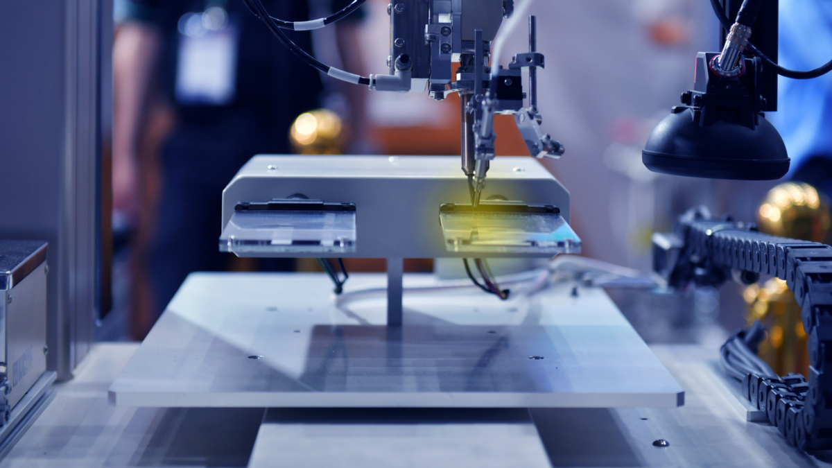
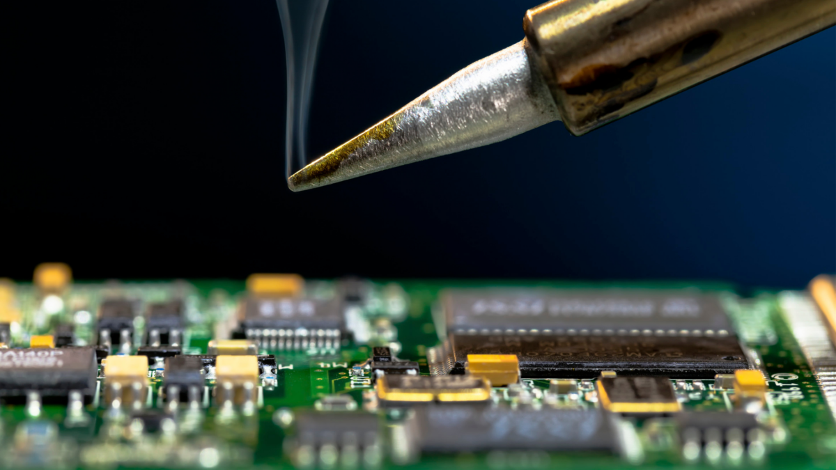
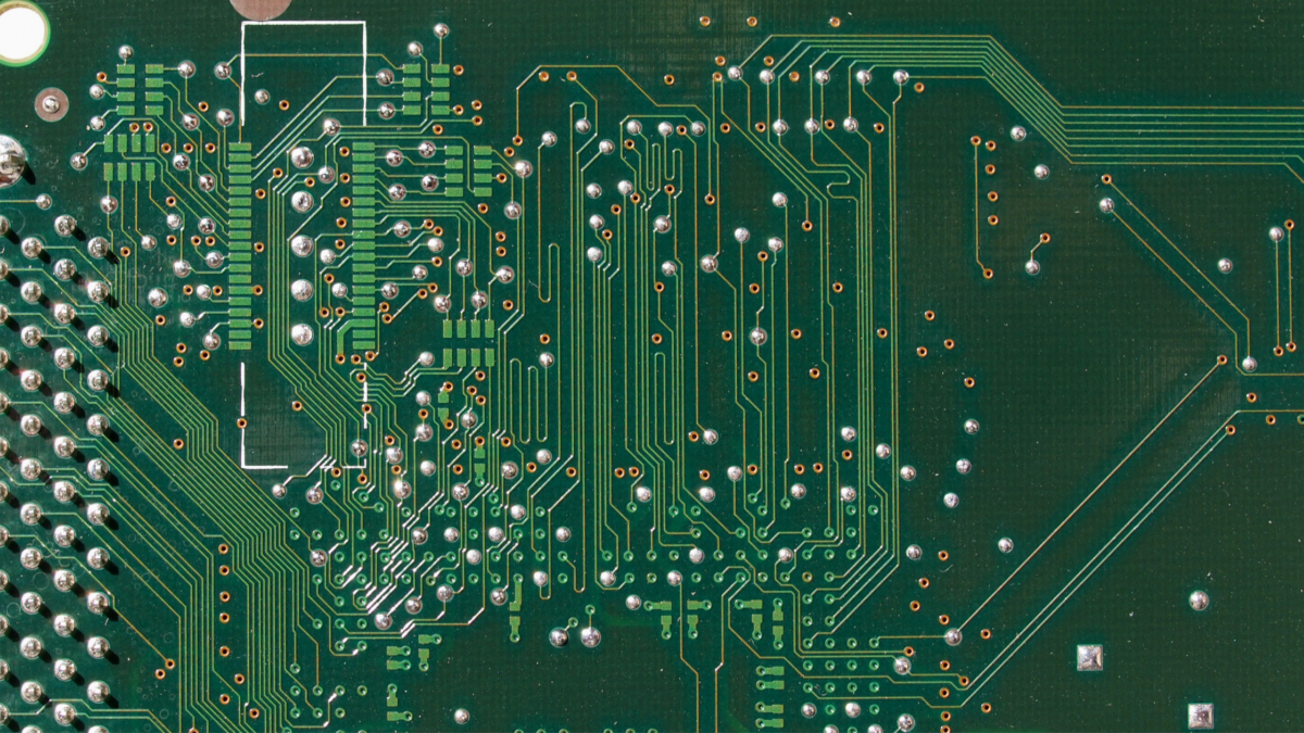
During the 1960s, double-sided circuit boards became common. One side held identification printing and the other housed electronic components. This further improved layout efficiency and performance.

Surface Mount Technology (SMT) and the Rise of Automation

One of the most important developments in the history of circuit boards came in the 1980s with the introduction of Surface Mount Technology (SMT). SMT allowed components to be mounted directly onto the surface of the board, removing the need for drilling holes as in traditional through-hole technology. This reduced assembly time, improved reliability, and enabled further miniaturization.

At Nova Engineering, our PCB assembly process includes both surface mount and through-hole technologies, depending on the specific needs of your design. Our experienced team has been at the forefront of innovation for over 35 years, and we’re proud to continue pushing the boundaries of what PCBs can do.

The Modern Era of PCB Assembly

Today, PCBs are incredibly advanced. They often include multiple layers, solder masks, silkscreens, and precision-machined traces. Materials such as fiberglass, copper, and gold plating are commonly used. Whether it’s in smartphones, medical devices, or aerospace systems, modern PCBs are the silent workhorses behind the world’s most sophisticated technology.

With the rapid growth of Internet of Things (IoT), artificial intelligence (AI), and wearable devices, the history of circuit boards is still being written. PCB design and assembly must now meet increasingly complex demands, including ultra-compact designs, high-speed data transmission, and energy efficiency.

Nova Engineering: Proud to Build the Future

At Nova Engineering, we honor the history of circuit boards by delivering exceptional service in PCB assembly, including turnkey, consigned, and partially consigned builds. With three fully equipped production lines and a dedicated prototype line, we welcome projects of all sizes and complexities.

We’ve partnered with customers for over three decades to build the technology they’re passionate about. Our strong vendor relationships and expert team ensure competitive pricing and unmatched quality.

If you’re ready to bring your next PCB project to life, contact Nova Engineering today to request a quote.

The Future of Circuit Board Assembly: Top 5 PCB Trends of 2025

As technology advances, the future of circuit board assembly is rapidly evolving. Emerging innovations and increasing demands for efficiency, sustainability, and miniaturization are shaping how PCBs are designed and manufactured. At Nova, our team in Denver, Colorado, is dedicated to staying ahead of these changes, offering turnkey assembly, consigned assembly, and high-volume production to meet the needs of modern electronics.

What emerging technology and industry shifts will define 2025 PCB trends? Here are the Top 5 PCB Industry Trends shaping the future of circuit board assembly.

1. Miniaturization & High-Density Interconnects (HDI)

Smaller, more powerful devices drive demand for miniaturized PCB designs with high-density interconnects (HDI). As consumer electronics, medical devices, and aerospace technology shrink in size while increasing in functionality, PCB manufacturers must adopt advanced surface mount technology (SMT) and microvia techniques to fit more components in smaller spaces. Nova specializes in precision placement and compact layouts, ensuring optimal performance without sacrificing durability.

2. Automation & AI-Driven Manufacturing

Automation in PCB assembly is no longer a luxury—it’s a necessity. AI-powered automated optical inspection (AOI) and robotic soldering are transforming PCB assembly trends, enabling faster production, fewer errors, and higher efficiency. AI-driven analytics optimize workflows, reducing waste and improving quality control. At Nova, we integrate cutting-edge automation to streamline production, ensuring high-volume orders meet the highest industry standards.

3. Flexible & Wearable Electronics

The growing market for wearable tech and flexible electronics is pushing PCB manufacturers toward flexible and rigid-flex PCBs. These boards, made from polyimide or other bendable substrates, allow for curved and adaptable designs used in medical wearables, smart textiles, and automotive applications. 2025 PCB trends will see increased demand for flex-rigid PCB solutions, and Nova is well-equipped to deliver high-quality flexible circuits that meet durability and performance requirements.

4. Sustainability & Eco-Friendly Materials

As industries shift toward greener practices, sustainability is a critical factor in the future of circuit board assembly. The push for lead-free solder, recyclable PCB materials, and energy-efficient production processes is stronger than ever. Companies investing in sustainable PCB assembly will gain a competitive edge, reducing environmental impact while meeting regulatory standards. Nova is committed to eco-conscious manufacturing, sourcing high-quality, sustainable materials while optimizing processes to minimize waste.

5. Internet of Things (IoT) Integration & Advanced Connectivity

With billions of IoT devices expected by 2025, PCBs must support low-power consumption, wireless communication, and high-speed data transfer. IoT-driven applications require PCBs with multi-layer stack-ups, embedded sensors, and enhanced RF capabilities. Nova specializes in designing and assembling IoT-compatible PCBs, ensuring seamless connectivity and efficiency for smart home devices, industrial automation, and medical monitoring systems.

Looking Ahead: The Evolution of PCB Assembly

The future of circuit board assembly is defined by miniaturization, automation, flexible electronics, sustainability, and IoT-driven designs. To stay competitive, manufacturers must embrace innovation and adapt to the latest PCB assembly trends. At Nova Engineering, we leverage over 35 years of expertise, cutting-edge production lines, and a commitment to quality to help our clients bring their products to life.

Whether you need turnkey assembly, consigned assembly, or a high-volume production partner, we’re here to help. Let’s build the future of electronics—together.

Ready to take your PCB assembly to the next level? Request a quote today!

Top 5 Latest PCB Board Assembly Equipment

The process of assembling a PCB board has become both increasingly precise and technologically advanced. Whether you’re just starting to build a PCB board or you’re working with an established assembly company, the latest PCB board assembly equipment can take efficiency and accuracy to the next level. With each new breakthrough in assembly technology, the process becomes faster and more reliable, providing the foundation for cutting-edge electronics.

Here’s a rundown of the essential equipment needed for PCB board assembly in 2024:

1. Solder Paste Printing Machine

In PCB assembly, applying solder paste is the crucial first step. This paste, often a mix of tin, lead, and silver, acts as an adhesive, allowing components to securely bond to the board. The solder paste printing machine ensures a precise and consistent application of this paste onto the board’s SMD pads through the use of a stainless-steel stencil.

Today’s solder paste printers come equipped with enhanced precision capabilities, driven by AI algorithms that adapt to each board’s layout. These machines minimize waste and guarantee that solder is applied uniformly, which is vital for the success of the entire assembly process.

2. Advanced Glue Dispensing Machine

To avoid component displacement during reflow soldering, glue dots are strategically applied to the board using a glue dispensing machine. With the rapid pace of modern PCB board assembly, this machine is more critical than ever, especially for double-sided boards where components could otherwise fall off due to gravity or the force of the solder wave.

The latest glue dispensers offer adjustable speed and dispensing pressure settings, allowing manufacturers to customize glue application based on component size and layout. These features help avoid glue overflow, which can interfere with soldering and affect the functionality of the finished PCB.

3. High-Efficiency Reflow Soldering Machine

Reflow soldering remains the most widely used soldering method in PCB assembly. This process involves heating the PCB in a reflow soldering oven, where it passes through zones of increasing and decreasing temperatures. The latest reflow soldering machines feature sophisticated thermal profiling, which prevents overheating and ensures a solid bond between each component and the PCB.

Advanced models now use machine learning to monitor temperature zones and predict any potential issues before they arise. This innovation reduces the chance of defective boards and shortens the overall assembly time, which is especially valuable for large-scale PCB production.

4. Automated Optical Inspection (AOI) System

As PCB designs grow in complexity, thorough inspection becomes essential. Automated Optical Inspection (AOI) systems have become indispensable in identifying defects early in the assembly process. Modern AOI systems utilize high-resolution cameras, laser measurements, and AI-driven pattern recognition to detect issues with unmatched accuracy and speed.

The latest AOI systems in 2024 can identify even the subtlest irregularities, such as micro-cracks, tombstoning, and misalignments, which would be impossible to detect with the naked eye. These systems reduce the risk of defects reaching the final product, saving both time and material costs in the long run.

5. Functional Validation Test (FVT) Systems

Once assembly is complete, the Functional Validation Test (FVT) checks that the board performs as intended in its real-world application. Unlike earlier inspection methods, which only focused on physical flaws, FVT involves loading software onto the PCB and testing its performance within the end product environment.

The latest FVT systems offer modular testing capabilities, allowing manufacturers to quickly adapt the test parameters to different PCB designs. This flexibility is particularly beneficial as custom PCBs become more common, enabling tailored testing solutions that match the board’s end-use application.

Crafting Perfection: How Advanced Machines Revolutionize PCB Assembly

As the industry advances, manual soldering and assembly are becoming increasingly rare for large PCB production runs. With innovations in PCB board assembly equipment, companies can now build a PCB board faster and more accurately, minimizing errors and maximizing reliability. For businesses in need of high-volume, high-quality assembly, these cutting-edge machines deliver precision that meets the demands of today’s sophisticated electronics market.

How to Print Circuit Board with PCB Assembly Process

Our daily lives are completely dependent on electronics. Electronic components are present in everything, from our cars to our smartphones. The printed circuit board (PCB), also called the brain of these electronics, is at its core.

The majority of individuals can identify printed circuit boards when they see one. You’ll find these tiny chips covering copper and lines components at the centre of disassembled electronic gadgets. These boards are made of copper, fiberglass, and other metal components. They are joined together by epoxy and solder-masked for insulation, and this solder mask is the source of their distinctive green hue.

Let’s explore the process of printed circuit boards with the PCB Assembly Process.

Step 1: Solder Paste Stenciling

You have to apply solder paste on the board as the initial step in making PCBA. Except for using a mask, this procedure is similar to one used for shirt screen-printing. Consequently, only certain sections of the potential PCB can receive solder paste application from assemblers. The assemblers apply the solder paste where they have to place the components.

Step 2: Pick and Place

With the help of pick and place device, the PCBA process continues. Pick and place device installs mounting components or SMDs on the PCB. If you see a PCB, you will find that most non-connectors are SMDs.

Step 3: Reflow Soldering

After assembling, the assemblers ensure that the components and solder paste stays in place. Therefore, they let the solder paste dry before placing the components. Reflow is a technique used in PCB assembly to achieve this.

Once the pick and place procedure is finished, the PCB board is moved to a conveyor belt. A huge reflow oven—which resembles a commercial pizza oven—passes down this conveyor belt. The board is gradually heated to about 480 degrees Fahrenheit or 250 degrees Celsius in this oven, which is made of several heaters. This temperature will cause the solder in the solder paste to melt.

Step 4: Inspection and Quality Control

It is necessary to test the constructed board for operation once the surface mount components have been soldered during the reflow process. This does not signify that the PCBA has been completed. The movement during reflow frequently causes a connection to be of poor quality or lost entirely. This movement can occasionally result in misplaced components connecting parts of the circuit that shouldn’t be connected, leading to shorts, another frequent adverse effect.

Step 5: Through-Hole Component Insertion

Besides SMDs, there are other components on the board. But, the number of other component depends on the board’s type.The most popular type of PCB process is plated through-hole.

A PCB hole fully plated throughout is known as a plated through-hole.The holes help PCB components to transfer signals to the entire board. It is not possible to use soldering paste on this section of the board because it flows inside the hole without creating a bond between components.

Step 6: Final Inspection and Functional Test

After soldering, you have to conduct a test to check the capabilities of the board. A “functional test” is what is being performed here. This step evaluate the performance of the board while imitating the typical operating conditions. The PCB is exposed to the simulated signals and powerin this test while testers observe electrical properties.

Conclusion

The most effective method for cleaning residue off PCBs is to use a stainless-steel, high-pressure washing machine with deionized water. The gadget is not at risk while washing PCBs in deionized water, so the actual water itself—rather than the ions it contains—causes harm to a circuit. As a result, PCBs can be washed in deionized water without harm.

Circuit Board Assembly – Step-by-Step Guide

Printed circuit boards or PCBs may look complicated, but that may not be the case. Simply put, PCBs are nonconductive materials with holes or pads designed on them. These holes help mount electrical components on them. 

Along with mounting holes, they also have small embedded connections that you call traces. Traces act as wires, connecting the electrical components together and allowing them to function cohesively, which is critical for an electrical appliance’s functionality.  

To understand the assembly process, you must know the basics of a printed circuit board. 

PCB Basics

First, you should know that there are two ways to attach a component to a circuit board: the surface mount method, or SMD, and the Through Hole technique. In the surface mount technology, you have copper pads on the board, and you have to lay the components on top of them. 

You then have a through-hole technique where you stick the ends of a component through the board and then solder them from the bottom. If you are new to PCBs and not skilled at soldering, the through-hole technique is the way to go. However, the components tend to be bigger, so you will not be able to create a compact design. 

Below, we will discuss the step-by-step PCB assembly process on a large scale. 

Soldering 

The assembly process starts with soldering to the circuit board. The machine carries out an inspection at the start, in which it inspects the circuit board and ensures it is aligned. Once it is aligned, the machine will apply solder across the board’s surface evenly and smoothly. The machine ensures that the solder comes in contact with all the pads.  

Pick and Place Machine

After soldering, the next assembly step requires the board to go to the pick-and-place machine. You must use a manual process for a low-volume prototype assembly, so you must place the board inside annually. The pick-and-place machine select’s it’s tools and then collects individual parts to place them on the board for rapid succession. After the pick and place process, the board is ready to refloat. 

The head that moves back and forth on this machine can hold eight components simultaneously. The parts that come from reels include the tape and reel board. The head travels and picks up over eight parts at a time from the reels and advances them so that the next part is ready. 

Refloat Process 

Refloat process is crucial because the solder needs to melt for adherence. This will make the board good for both mechanical and electrical connections for all the parts. It travels across the big machine and comes out from the other side after being cooked. Once the solder cools, junctions between each part come into creation. 

To Conclude

After the surface mount assembly, you can install through-hole components and create beta appliances. As you can see, manufacturing a printed circuit board involves a step-by-step process and careful considerations. The assembly process can, however, vary according to the size of the board and its electrical components.

As you can see, the PCB manufacturing process requires state of the art machinery and qualified expertise. If you want your printed circuit board assembly to be highly efficient and functional, you should look for a good manufacturer. Expert manufacturing companies are thorough with their design and assembly process, and can pave way for excellent appliances thanks to their sleek design. 

How To Solder On Printed Circuit Boards

Solder is a material that manufacturers use in the printed circuit board assembly process. This material can join soft metals such as gold, copper, and silver together. Copper is the common material in the printed circuit board assembly or any electronic item.

Most commonly, manufacturers will use eutectic solder, a combination of tin and lead. This is about 63% and 37% lead, and it comes with a formulation with a minimum melting point for the combination of metals.

Properties

Different solders come with different melting points and ranges of temperatures where solid and liquid tend to co-exist together. You can also form a pasty substance as it cools, and you can find that it is very flexible. The flexible property or ductility allows the metals that join it to interpenetrate once you melt it.

It is a dense and heavy material because it has a high lead content. It also comes in several different gauges and wire diameters. For surface mount devices, a very fine one is more useful. You can also find lead-free, which comes with the formulation of tin, silver, and copper.

This does have a melting point, and you can use this commonly with electronics that use low-temperature soldering irons. Lead-free has a high melting point, which is why it can be difficult to work with. This material is also relatively new, and most people will be unfamiliar with its properties.

Printed Circuit Board Soldering

A printed circuit board holds electronic components and provides a mechanical means of holding them in a space where they connect electrically. A printed circuit board contains different resistors, active circuits, and capacitors.

The circuit board holds them together collectively and consists of several layers. The first layer you see is a green layer, a polymer called LPI. This photo image-able polymer can go down as a liquid and dry to form a solid layer. The green layer is necessary to prevent it from crossing over and shorting traces that should not connect.

Basic Technique

If you are manually soldering components to a printed circuit board, you must adhere to the basic technique. There are two different types of soldering iron. One has a station that controls and adjusts the desired target temperature. The other melts electronics at a fixed temperature, which you can use similarly.

Soldering iron heat up and melt the solder on the circuit boards. When it melts and cools on the printed board surface, it cools and solidifies, fusing to the surface of the metal at a molecular level and enabling electrical conductivity within the two metal platforms.

When soldering with an iron, you can also use flux, which helps it to flow, and also provides good contact by removing oxides on the surface of the metal. Although modern flux is not toxic, you should always use a fume extractor.

Two Different Connections

You can find two different types, surface mount and through hole. Surface mount connections require manufacturers to heat components in an oven with pre-applied. This allows it to melt and join to the board’s surface. Through-hole is when you push the components through the printed circuit board hole and solder them from the other side. The solder travels across the hole to make good contact.

Final Words

As you can see, this is an essential part of the printed circuit board assembly process. It is best to resort to a professional manufacturing unit to do a perfect job. The best soldering service will use top-notch technology for clean and precise solder.

How Do You Define a PCB?

This post will talk about one thing only: Printed Circuit Boards, or PCBs for short. You must know that the world of technology keeps expanding as new devices, gadgets, and equipment make their way into our lives. What keeps the electrical appliances and equipment running? Is there a core component without which your electrical device, like a smartphone, laptop, or vacuum cleaner, won’t work? Yes!

Printed Circuit Boards are the core components of many electrical devices. In technical terms, a PCB creates conductive pathways to connect and mechanically support electrical components. We won’t be talking in purely scientific and mathematical lingo – don’t worry! Let’s find out what a PCB refers to and what it does.

What Do You Define a PCB in Technical Terms?

Here’s how you define a Printed Circuit Board or PCB:

“A PCB forms the board base for connecting and supporting multiple electrical components using the surface mount technology to run electronic products.”

Have you ever accidentally cracked open your phone or even an electronic toy? Did you see a green electric board with numerous wires attached to different parts of the individual item? Well, that’s a PCB! It has socketed or open components that transfer electrical signals and conductive traces through conductive pathways to run an electronic product.

Like animal and plant cells require a nucleus at the center to function and coordinate other mechanisms, nearly every electronic product requires circuit boards. A more technical term for circuit boards is “printed circuit boards”. Many standard devices like laptops, smartphones, and even vacuum cleaners won’t work without it.

How Do Factories Make PCBs?

PCBs are electrical circuit boards in various shapes, sizes, and designs. Since they fit many electronic product categories, they are not the same. Factories are the production houses where electrical circuit boards get fused with electrical components to produce PCBs!

Every PCB is different yet vital to the functionality of the device it’s for. The most standard version is a plastic board covered with fiberglass. Having a non-conductive plastic board is essential to make a high-quality board. The manufacturers create small conductive pathways on that board to mount and connect multiple electrical components.

The conductive traces (pathways) assist components in passing electric signals through it. It contains numerous holes to fit each component. First, manufacturers add a soldering paste to the board, passing it through the “pick and place” technique where components are attached to it.

Second, it goes through the soldering process to permanently attach every component to the board. Then, the board goes through physical and functional inspection (testing phase) to ensure high-quality production. Finally, the factories receive test feedback and performance reports before readying them for supply to the market. 

What Happens When a PCB Corrupts or Malfunctions in a Device?

Printed Circuit Boards are the core components of electronic devices. So, when the board takes out or if it malfunctions, the device will probably stop functioning. Even if a single important component malfunctions on the board, the whole device could malfunction or stop working altogether.

Fixing it as soon as it gets damaged or malfunctions is the best approach, especially when it’s an essential household or personal device like a smartphone or laptop. There could be dozens of issues and reasons behind a PCB not functioning correctly, including:

  • Poor soldering
  • Low-quality soldering paste
  • Damage in the assembling process
  • Heat-up issues
  • Poor-quality components 

Conclusion

You will only have a limited range of electronic products if factories stop producing electrical products, mainly printed circuit boards. You can only imagine how far the effect of PCBs travels in our daily lives. PCBs are in numerous devices, from personal hygiene products to military equipment and navigational systems.

The Right Way to Solder on Printed Circuit Boards

Soldering is the most vital part of the PCB assembly process. It’s where the electrical components get attached to circuit boards. Without electrical components, no PCB would function effectively. There are various methods to sell electrical components to PCB and ensure electrical currents pass through the conductive pathways efficiently.

The main issue is that many people don’t know the right way to solder electrical components on circuit boards. Since a bunch of them are being used in factories, it can be quite tricky to pick the right one. We will discuss some of the top soldering techniques so you can choose the one that’s right for your business.

The Right Way of Soldering on Printed Circuit Boards

In the electronics world, soldering is a fundamental skill that nearly every professional must have at some point. Soldering and electronics go together like a fork and spoon.

Although people learn how to design, build, and release electronics without picking up a soldering iron, it’s still a vital part of the industry. Let’s check out a few soldering methods and techniques commonly used these days.

1.      Reflow Soldering

It’s the most common soldering method factories use today, especially for manufacturing surface mount technology or SMT printed circuit boards. This soldering method involves using a heated soldering paste to attach electrical components to the circuit board. The paste looks like molten metal, enabling professionals to connect pins and pads seamlessly. However, it results in permanent attachment.

2.      Wave Soldering

Wave soldering was once extremely popular for wave soldering. However, it’s still commonly used for surface-mount technology circuit boards. Printed circuit boards that go through the through-hole process (i.e., drilling holes in the board to fit electrical components) usually also go through the wave soldering process.

Generally, factories utilize wave soldering to produce massive PCB assemblies. The PCBs go over molten solder in a pan that looks nothing less than a wave pool. Once through, electrical components get attached to the circuit board.

Before coming in contact with the molten solder, the components are already glued to the board. Due to an additional step that reduces efficiency and somewhat increases the time and money consumption, reflow soldering replaced wave soldering.

3.      Braze Soldering

Soft and hard soldering is nothing compared to brazing. Brazing results in fortified joints between the printed circuit boards and electrical components, including transistors, inductors, and capacitors. It uses high temperatures to attach electrical components to circuit boards.

Although it’s similar to hard soldering (discussed later), brazing involves melting the underside of the metal components to get attached to the board. It causes the least thermal deformation and is one of the best soldering techniques for mass PCB production.

4.      Soft Soldering

Soft soldering is the perfect option for compact and fragile circuit board components. Soft soldering doesn’t damage the electrical components through high heat or molten solder. In this process, the temperature of the molten solder is below 400 degrees Celsius or 752 degrees Fahrenheit.

If the temperature goes over, it becomes “braze soldering”. The low-temperature technique is for smaller components prone to breaking at high temperatures or heat conditions. Although it’s suitable for small components and fragile boards, it doesn’t produce the strongest joints.

5.      Silver Soldering (or Hard Soldering)

This soldering technique also yields strong joints between components and circuit boards. However, combining metal components such as gold, silver, or brass-plated components is best. It’s used to connect and attach the same metals in other industries.

Conclusion

What type of printed circuit board you’re producing will determine the right soldering technique. Other factors influencing the soldering technique include existing capabilities, materials, and requirements.

Check which soldering technique offers the most lasting results and try to match it with your PCB requirements. Partnering with a solid PCB manufacturing company could ease the process and increase soldering efficiency.

What Goes Into The PCB Assembly Process?

The fast-paced technology around us brought countless electronic devices and equipment into our lives. Those electronic items have PCBs at their core. This post is for you if you don’t know what PCBs are. Just like a living cell has a nucleus at its center, Printed Circuit Boards are present in nearly all electronic equipment and devices.

Manufacturers use the “pick and place” technique to assemble and produce PCBs based on Surface Mount Technology or SMT. PCBs are small green boards that have electrical components on them. The components get attached through soldering to make the final version of a PCB. Simply put, designing, layout, printing, soldering, and testing a board is the “PCB assembly process”.

What Goes Into the PCB Assembly Process?

The process involves various steps, including soldering, pasting, designing, and testing. In this section, we will look at those processes in a systematic sequence to give you a better idea of PCB assembling.

Reliable manufacturers align the processes with above-average standards to produce high-quality PCBs. As the vast majority of PCBs feature the surface mount technology these days, the process below is for the same type of PCBs:

  • Solder Paste

Before adding any components to the printed circuit board, manufacturers add solder paste to it. The paste is only for the component pads, i.e., only the spots that will have components on the board. It’s done using the solder screen and protective machinery.

  • Pick and Place Technique

The board with solder paste goes through the “pick and place” process. A machine containing components places them on the printed circuit board. The machine does that very carefully to ensure proper placement and in the correct position. The tension between the components and solder paste keeps them attached to the board, considering you don’t jolt the PCB too hard.

  • Soldering

After adding components following the solder paste, the boards go through the individual soldering process. That’s where the soldering machine will permanently solder each component to the board. However, this process isn’t widely popular with surface mount technology-associated PCBs anymore.

If the manufacturer uses the wave soldering machine, the first step of the assembling process will be the pick and place technique. The board won’t require solder paste separately as the wave soldering machine provides solder paste. However, reflow soldering is more popular than wave soldering for assembling PCBs.

  • Inspection

Without inspection, reliable manufacturers don’t release PCBs into the market or supply them to their business clients. Inspection deals with issues that might have developed at various stages of the assembling process. PCBs with surface mount technology have dozens of components and sometimes a hundred. Hence, manual inspection is time-consuming and discouraged.

Automatic optical inspection is a more feasible solution for surface mount boards. The optical inspection machines scan and detect poor joints, abnormal soldering, and inappropriate placement. It catches both visible and non-visible issues with the surface mount.

  • Testing

Once the inspection and correction are over, the PCBs go through the testing phase. Before leaving the manufacturer’s den, testing PCBs is necessary to ensure they’re functional and suitable. Factories use different ways to test PCBs and surface mount boards.

  • Feedback

At the end of the process, the manufacturers receive reports to monitor the overall production quality, especially concerning PCB quality. Factories check for issues and monitor the functionality of PCBs during the testing phase to know they’re producing high-quality printed circuit boards. 

Conclusion

All PCB manufacturers rely on quality and safety standards to deliver reliable printed circuit boards. Furthermore, many types of PCBs are on the market to fit various electrical devices and equipment.

Learning about the PCB assembly process enables you to find the right manufacturer based on your requirements. If you’re developing electronics or similar goods, you’ll require an extensive insight into the assembling process to use the perfect PCBs for your projects.

Why Surface Mount Technology is Better Than Conventional Technique

The standard practice for manufacturing PCBs involved through-hole circuits. It’s a simple method and refers to cutting holes in the circuit board to fit electrical components as required. However, it can be very time-consuming if used for mass production of through-hole PCBs.

Machines drill holes in the boards, mount components over those holes from one side, and then thread the holes in the board using lead. Since innovation leaves no technology untouched, the through-hole practice became obsolete only a few years after surface-mount technology or SMT took the stage.

Surface-Mount vs. Conventional Technique: Benefits of SMT 

It was the solution manufacturers wanted. SMT enables manufacturers to produce PCBs at high speed and with more material efficiency. Furthermore, it brings adequate vibration resistance and the possibility for customized soldering techniques. Let’s take a broad look at how SMT transformed the world of electronics and PCB production practices.

  • PCB Miniaturization

The electrical components attached to circuit boards using the surface-mount technology are much smaller than through-hole interpolation components. The geometric volume and size differences in conventional and SMT techniques take PCB miniaturization to the next level.

The SMT technique has reduced the size of many electrical components by 60% to 70%. Over that, some components even got reduced to 90% of their size thanks to surface-mount technology. The same goes for the weight. Hence, with SMT, PCBs have become smaller and more lightweight.

  • Low Material Costs

You will see a significant difference when you compare the material costs of conventional PCB manufacturing techniques and surface-mount technology. Considering the miniaturization that SMT brings into the PCB world, the material costs are significantly low.

Since small PCBs have smaller components, the material costs reduce automatically. In turn, that drives the price of SMT PCBs downwards, making it a more favorable option in electronics.

  • Simplified Production Processes

The surface-mount technology simplifies the production process to a massive extent. For instance, the mounting technology requires manufacturers to bent, shape, and cut the electrical components before mounting them on the circuit boards.

That automatically reduces the time, energy, and money spent attaching components to the circuit boards. Hence, the process simplifies, making it far more manageable and less time-taking.

  • Better Production Efficiency (and Automatic Production)

Surface-mount technology pioneered automatic PCB production processes in factories. It involves standardization and serialization in the production process. Moreover, it also brings consistency to the welding processes for attaching chip components to SMT printed circuit boards. Thus, the reliability of compact components on miniature PCBs will increase while the rate of component failure reduces gradually. 

  • Improved Signal Transmission Speed

Do you know that SMT brings higher safety density to PCB structures? Although the technology created miniature printed circuit boards, it also improved the safety density. For instance, the solder joints per cm2 can be around 5.5 to 20 as assembly density.

You must realize that high signal transmission speeds will also increase PCBs’ resistance to impact and vibration. This could ultimately result in high-speed operations and better electronic equipment around us. 

  • Better High-Frequency Effects

The distributed parameters of the circuit boards are generally high. However, they reduce drastically when the components attached to the board either have no or short lead. That’s because the absence or negligible amounts of lead causes reduced RF interference.

Conclusion

Learn about printed circuit boards and your requirements before choosing surface-mount technology. You will require thorough analysis and proper planning for successful end-product manufacturing if it includes PCB.

And if you’re planning mass production, make a prototype for testing. With surface-mount technology, you can create simpler designs and compact devices with quicker completion times. However, considering your requirements is best to do a cost-benefit analysis.

How is PCB Made in China?

Circuit boards are the heart of just about any piece of electronic item that you use. China is responsible for a big chunk of the world’s circuit board production. In hindsight, printed circuit boards are a specific assembled product, even though they may look very complicated. The United States have largely relied on China for PCB production, but there seems to be a re-shoring trend underway.

The Re-Shoring Trend

Re-shoring is the act of having production units that were outsourced at foreign locations back to your hometown. US PCB companies have been setting up production units back to their hometowns and shutting down operations in other countries. The reason for this move is the increasing amount of labor costs in other countries, paired with the prevailing supply chain issues that are slowing down delivery times.

Not only that, due to the Geopolitical tensions, US citizens now demand that the products they consume are natively built. There is also a threat of intellectual theft when you hand over technical operations to other countries. Taking all of these existing factors into account, the re-shoring trend has become evident.

Below, you can get a glance of the technical process.

The Very First Step

Before a design file can be put into production, engineers will first glance at the file to ensure there are no inconsistencies within the design. Engineers need to check things such as trace gaps, files, drills, and other aspects of the digital PCB design they receive. This will ensure that the engineer did not design the PCB in a way that you cannot manufacture it.

Printing the Design onto Film

Once the design is reviewed and corrected, the design will then turn into films. You can make films and use light to project an image onto a board with a photoresist. This is similar to how you would expose a photograph. Once you have the design, you need to transfer it onto a copper board blank. Before you can shift the film onto the blank board, manufacturers will first prepare the board.

Board Production

The PCB board is manufactured using a layer of fiberglass in between and then gluing copper on the outside. In a large-scale manufacturing unit, large sheets of blank PCB boards are cut down into smaller components. After the board is cut, it is sent to the drilling unit. There are two reasons manufacturers drill a printed circuit board.

The first is to connect the components, and the other is to accommodate the wire holes connecting the copper layers. To begin with the drilling process, an operator will take an MDF board as exit material.

They will then attach an aluminum sheet on top of the board, which acts as an entry for the machine drill. This machine is fully automated, allowing it to select the right size of the drill. After doing so, it loads it into the drill head.

Most PCB manufacturing units in China will use highly optimized drills that can rotate up to 15 thousand revolutions per minute. After that, the corners are trimmed to make them rounded, and the surface is cleaned. Then, the machine automatically smoothens the edges of the board.

Final Steps

The steps that follow allow the board to go through a series of processes where copper is plated, and a printer prints photosensitive film to the copper board. Once the film is attached, further mechanical processes and solder masking will lead to the completion of the printed circuit board.

The solder mask protects that copper surface. The attachment of the components and testing is done with the help of machines. After the testing is complete, workers will separate all individual PCBs from the large production panel.


How to Repair Broken Traces on a Circuit Board?

Different methods can help you repair broken traces from a circuit board. Today, there is a prevailing shortage of microchips that are microprocessors. Traces are what connect microchips and all other essential components on a circuit board.

Damages on Traces

Traces on a circuit board are not new to damage. They can suffer from damage in several ways. They can get damaged due to accidents or even due to dirt or residue. Most of the time, damage on the PCB traces is due to corrosion. Corrosion can happen because there is a leak in the electrolytic capacitor or a leak in the batteries. They can also be caused due to poor storage. To repair broken or damaged traces on a circuit board, you will first need certain tools and equipment.

What will you need?

To start with, you are going to need a soldering iron. Remember that your soldering iron does not have to be the best in the market. However, it is recommended that you have a soldering station rather than just one soldering iron. Along with that, you will need a high-quality gel flex and a very good set of precision tweezers.

You will need a blade, scalpel, or sharp object for cleaning, and a UV solder mask, along with solder, for reapplication. Do not forget that you will also need some wire for the actual trace repair. Afterward, you will need some isopropyl alcohol and some q-tips, cotton buds, and a toothbrush.

It is also very good to have multimeter so that you can keep a check on your work progress. Not to mention, a multimeter will be beneficial because it helps you keep a check on your work to make sure you’ve renewed continuity in the damaged traces.

Other things you’ll need include very sharp eyesight and a steady pair of hands. If you don’t have good eyesight, it is always a good choice to use a microscope. A microscope is an effective way to se what you’re doing without making errors.

You can even connect a camera to this microscope to enhance your work. Since a microscope can be pricey, they are not easily available. In this situation, a magnifier is a better alternative when trying to repair broken traces on a printed circuit board.

Use Enameled Wire

You should use enameled wire, the same type of wire you would use on a transformer or an electromagnet. It has an enameled coating, which means that it is insulated, making it very functional inside a printed circuit board. Nonetheless, this enameled coating comes off very easily with the heat of the soldering iron.

So if you need to run a trace over the board where it might come in contact with other metal, the insulation will stop it from creating a short. As you can see, repairing broken traces on a printed circuit board requires extensive consideration and thought, and you must be willing to take all the precautions to do a clean job.

To Conclude

With careful consideration and some knowledge of printed board repair, you can easily repair the broken traces on a printed circuit board. The above-mentioned types of equipment can help make the repairing process easier. All you have to do is spot the broken trace, clean the corrosion, and apply new wires on them with the help of solder.

Why Is The PCB Manufacturing Process So Essential?

When trying to understand how a printed circuit board works and its application, it’s essential to know the manufacturing process. Learning about the manufacturing process of PCBs can help you gain a more insightful understanding of the circuit board’s functioning. The manufacturing process for printed circuit boards introduces you to some of the most fundamental concepts of the PCB design.

Basic Board Structure

The PCB consists of multiple layers, and these layers also impact the manufacturing process. The critical layers of the printed circuit board include the copper layers. These are where you will find the traces. The traces are the wires within the circuit that connect the different components.

In a two-layered circuit board, you will have a top copper layer and a bottom copper layer. Between the two layers, you will find a dielectric material that is made of fiberglass. This fiberglass material is also called the Substrate, and engineers often refer to it as FR4.

In addition to that, most boards also contain a layer that sits on top of the copper, as well as on the bottom of it. This layer is called Soldermask, and it is a critical aspect of the PCB manufacturing process.

Soldermask

Soldermask is a layer of insulation that sits on top of the copper so that the components on the board are not in contact with each other. Very often, you can also find a layer of silkscreen on top of the printed circuit board. This silkscreen is text that allows you to identify the components inside a PCB.

The solder mask is the green layer of material that you find on PCBs. Whenever you have exposed copper on the PCB, you can apply a solder mask to it. The manufacturing process also involves making holes inside printed circuit boards, called through-holes.

These holes are plated through the board, with copper all the way through. These are the sorts of things that manufacturers will typically solder through. There are other types of holes, and engineers will call them Via.

Vias connect a wire on one layer to another layer. If you look at a board carefully, you will have lighter green areas and darker green areas. Where you have lighter green areas, you will find copper sitting on top of the FR4 Substrate.

Silkscreen

Copper on a printed circuit board is effectively on a large plane and traces. The silkscreen sits on top of the highest layer, which gives the reflection of the lighter colors on the board. Darker areas on the copper are simply solder mask and Substrate.

Manufacturing a Multilayered Board

In a multilayered board, what you have is a sandwich of individual boards. In other words, creating a multilayered board will require you to stack one board on top of another. A motherboard inside a computer can have about 16 layers which are very complex.

The Significance of the Process

The PCB process is incredibly complex. It encompasses multiple steps, and there are incredibly large boards with multiple different designs that are flowing through the factory. In today’s world, highly automated and large-scale machines make it possible to produce high volumes of Printed Circuit Board in a single day. This simple phenomenon has expanded the growth of technological innovations around the world, giving way to the acceleration of mechanical and electronic progress.

Circuit Board Components and Their Applications

A PCB board or a circuit board is a critical component of almost all electronic pieces of equipment that are computerized and made to limit manual efforts. Even though they may look small and ordinary, circuit boards often have many complex components that synchronize to make a particular device function.

These components play a critical role in the functioning of a circuit board, which is responsible for the performance of all electrical items. Components attached to circuit board assembly can vary depending on the electrical appliance’s functions. However, some components are commonly found on all circuit board assemblies because they’re essential.

Resistors

Resistors are available in different shapes and sizes for circuit board assembly. A resistor is an electrical circuit that is meant to, as the name suggests, resist electric current flow. It is bound by Ohm’s Law, where voltage equals current multiplied by resistance. It encourages the restriction of electrical discharge. It is similar to how you narrow down a pipe to resist the amount of water flowing inside a tube.

Capacitor

There are all kinds of different capacitors, and they store charge in an electrical field. If you have a noisy electrical signal and voltage change, it will hold a charge and let some of the current out. It will then take on some charge when it reaches a peak. This means that you can smooth out a noisy signal with a capacitor.

Diode

The diode is the simplest semi-conductor. It allows the current to flow in only one direction and stops the flow if the current tries to flow in the other direction. LEDs or light-emitting diodes are different types of diode components on the printed circuit board capacitor.

Soldering the LED onto the printed circuit board is tricky, but it’s necessary when equipping a printed circuit board that powers an electrical component such as a mobile device. You can also find different sizes for LED parts.

Transistors

A transistor is a switch that has three leads. One of the leads is called the gate. If there is a current on the gate, electricity will freely flow between the other two leads. There are different types of transistors, some that only switch minimal loads, while others are bigger and can switch larger loads.

Micro Chips

Microchips are semi-conductors that come in every shape and size imaginable. They also start simple and get very complicated. Although it’s easy to solder them onto the printed circuit board by hand, they will perform much better when subject to machine assembly.

The contacts are underneath some of the chips and not easily visible. These types of semi-conductors are what you get if you take millions of transistors and put them together in the same package.

These microchips carry the majority of processing power in an electrical component. Different microchips are suited for different tasks, and it depends on the data they carry. The exact same chip can perform two different functions.

Final thoughts

The above-mentioned PCB components are some of the most critical and commonly found ones on circuit boards. Each one contributes to the flow of current around the printed circuit board, which is pivotal for the functioning of an electrical appliance.


Interesting Facts about Circuit Board Assemblies

PCBs or Printed Circuit Boards are major components of all electronic items. Normally, most people know very little about circuit board assemblies. A circuit board can easily be the heart of any electrical component. Below, you will learn about some interesting facts and history about the printed circuit boards.

PCB was Made Up of Brass

By using PCB, you can reduce the size of electrical components and wires that are needed for electronics to function. Since it is a replacement for all electronics and wires, you would normally think that a printed circuit board is made of copper. Even though this is true, it is worth noting that PCB was first made up of brass, and not copper. Today, they more commonly consist of fiber glass, composite 2 proxies, and other material.

PCBs Widespread Application and Forms

PCBs or printed circuit boards are also used in the printing industry. It is generally the backbone of modern day electronics. Circuit boards come in many different forms, and most PCBs are assembled using only a single layer. More sophisticated electronics and hardware such as motherboards, computer graphics or other cards can have multiple layers that sometimes can also go up to 12.

Even though PCBs are often linked with computers, they consist inside many other electronic devices, including radios, TVs, cell phones, and digital cameras. Along with their applications in consumer good electronics and computers, they are also applicable in a variety of other fields. The many different types of PCBs allow for them to be used in many other applications.

PCBs have different types

There are many different types of PCBs which you can find. These include:

  • Single sided PCB or Single Layer PCB
  • Double Sided PCB
  • Multilayer PCB
  • Rigid PCB
  • Flex PCB
  • Rigid-Flex PCB

 Single Sided PCB

Single sided or single layer PCBs are the cheapest circuit boards that you can find. These types only have one layer of the base substrate fiber glass. Furthermore, they also have one conductive copper layer. Electronic components for this PCB have holes that are not plated through. The compartments for the electronic components are on one side, while the conductive circuit is on the other side. Since there is only one conductive layer that forms this circuit, it is called a single sided PCB or one layer PCB.

Double Sided PCB or Double Layer PCB

Printed circuit boards of these types have one single layer of the base substrate, but conductive copper layer on both sides of the substrate. On this type of printed circuit board, you have to apply solder mask on both sides of the board. On top of that, holes for electronic components need to be plated through so that there is conductivity on both the circuits.  Holes on the double layer PCBs allow circuits on one side to be attached to circuits on the other side.

Multilayer PCBs

In this type, all the layers are interconnected with the help of copper plated holes. These layers can be multiple, and even range up to 40 layers. All the electronic components of an item are assembled on both, the top and bottom layers. On the other hand, the inner stacked layers are meant for rooting. Both, through hole electronic components and surface mount components can attach to either side of the PCB with the help of solder mask.

Final Thoughts

The earliest PCB assemblies were connected to each other manually, using wires. This manual construction led to errors and difficulties when it came to scaling up production. Today, printing techniques that conduct copper circuits on a non conducting board has revolutionized electronic items, making them smaller and more efficient.

How did Circuit Board Assemblies Evolve?

All inventions go through evolutionary courses. PCBs, or printed circuit boards, went through an incredible course in history. If there is one thing that has challenged the electronic assembly industry, it is the need for miniaturization. As components inside an electrical unit get smaller and closer together, it pushes the printing and cleaning process to the edge. One may think that miniaturization is a product of the last 5-10 years. However, this process began about a hundred years ago.

History of Circuit Assemblies

When you think of circuit board assemblies, you instantly think of them as modern technology. It all started with Albert Hanson, a German scientist who filed a patent for a device that would improve telephone exchange boards. This primitive circuit board had wires attached to a conductive substrate and bonded to a flat surface.

This device consisted of technology that you would consider a precursor to the modern-day circuit board. It also had the simple through-hole design of today’s circuit board. The first real circuit board came patented in 1927 by American inventor Charles Ducas. His circuit board design had stenciled conductive materials on a wooden board that was flattened out.

This may be how the word, “board” is incorporated into what you now call a circuit board. Charles Ducus utilized a stencil to print the wires directly onto the board. He also applied ink for the conduction of electricity. This concept aligned the electronic path to an insulated surface, which created a more recognizable device as a printed circuit board today.

Evolution into Multi-Layered Circuit Board

Ducus conceptualized his invention further and thought of the possibility of layering multiple boards, which will give existence to a multi-layered circuit board. However, connecting multiple boards into a multi-layered object would require another great inventor who had the capabilities to turn his concept into a reality.

Then came Paul Eisler, who is widely known and appreciated for inventing today’s printed circuit board. After leaving Australia in the early days of World War 2, he settled in England. He worked in a newspaper printing company, which led him to use his printing expertise to formulate an idea that printed electronic circuits onto boards.

This was a giant leap forward in the labor-intensive practice of hand soldering each wire manually. His inventions helped in World War 2 because they were used in radio sets that the British and Americans used during the war.

Etching Design

In 1943, a patent was issued for a circuit board design that was more advanced than the one used in World War 2. It involved etching the circuits onto copper foil and on glass-reinforced non-conductive substrates. In 1948, the US Army released this technology to the public so that it could prompt widespread development of the innovation.

Transistors

In the 1950s, the printed circuit board became subject to further enhancement as transistors emerged. These components helped reduce the size of the electronics and made it easier to incorporate PCBs into electronics. This also improved the reliability of the electronics, and it started the beginning of the long-driven goal of miniaturization. In the 1950s and 60s, PCBs evolved into double-sided boards with identification printing on one side and electronic components on the other side.

Concluding Thoughts

Today, printed circuit board designs have zinc plates, silicon chips, solder masks, and more components that make electronic components more effective. Moreover, the circuit board assembly technology known as the surface mount technology dominates the PCB world. Surface Mount Components are soldered directly onto the board and have become industry standard.

PCB 101

Circuit boards, which also go by the names, printed circuit boards and PCBs, consist of various electrical components. Comprising insulated board materials along with dozens of electrical components, PCBs feature different technologies ranging from surface-mounted to interconnected systems. They’re made for specific electronic circuits and perform a specified or a set of different actions.

Since their early development during the 1900s, the laminate materials on PCBs have gone through various developments and technological advances. Charles Ducas was the first to submit a patent for his circuit. The idea was vividly defined as placing a pathway comprising electrical components directly over an insulated material board. But, the real development and use didn’t find ground until after World War II.

Typical Use and Purpose of Printed Circuit Boards

In today’s modern world, just about every device has a printed circuit board. Nearly all electronic devices around us have some type of PCB or a combination of them to function effectively. In simple words, PCB technology was a ground-breaking development that paved the way for massive technological advancements to take place on a global scale.

The PCB technology is powering a range of applications and equipment across multiple industries. It’s safe to say that without modern printed circuit board production, research, and development, it wouldn’t be possible for massive innovations to take place in our technological space. Here’re a few uses and PCB’s modes of deployment around us:

Aviation

Aviation utilizes high-performance and lightweight PCBs to operate and design aircraft. Considering the size of the size of a typical PCB, that’s a humungous role that the technology is serving at the moment. From communication and drone construction to guidance systems, PCB technology offers lightweight and functional solutions.

Automobile

The automobile industry uses PCBs in a rather spectacular manner. The use of PCB allows automobile brands and manufacturers to place safety sensors inside vehicles! From keyless entry to ignition systems, PCB enables a range of different features in different makes and models of vehicles around us. Besides, the latest computerization of vehicles has stirred up demand for more intelligent vehicles.

Home Automation

The home automation industry is also utilizing PCB technology to assist in different features and other technologies. If you live in a home with a surveillance system, smart thermostats, and smart appliances, just about all of these technologies will have PCBs.

Entertainment

The entertainment industry probably has one of the biggest innovations that mankind has ever seen, thanks to PCB technology. It’s the development of flat-screen televisions. Humankind would’ve been stuck on fat monitors and TVs if PCBs didn’t replace the tube technology and wiring that was used previously. Even the miniature MP3 pods you may have used comprised of tiny PCBs that enable music playback and audio recording with wide variations.

Lastly, we don’t need to tell you what smartphones are, what they’re for, and how they’ve made our lives easier. However, it’s best to share that they comprise industry-best PCB technology to enable different functions and features that most users require regularly.

Latest Advances in the Technology

Here’s a list of some of the major advances in PCB technology, including fabrication techniques:

  • LDI, which stands for Laser Direct Imaging, is among the most precise ways to create PCB materials’ design images. It replaces the photochemical process that was too troublesome and usually inaccurate.
  • Flex PCBs technology allows greater flexibility in the fabrication of printed circuit boards. Thus, it’s easier to handle application-specific requirements when using PCBs in other technology-associated devices.
  • HDI stands for High-Density Interconnect Boards, is the main technology in use for efficient electrical component placement on insulated board material. It allows the placement of more components while requiring less space. Hence, it offers greater reliability and performance with reduced weight and space.

Conclusion

In the end, there’s a lot more to the PCB technology than just the recent developments and new fabrication techniques. Find out more through the latest research and studies to learn how PCB technology enabled a new era in modern technology.

Defining PCBs in New Light

Printed Circuit Boards or PCBs have evolved to become much more complex than before. Considering the early patenting and development, modern functionalities of devices featuring PCBs have improved to make them more intelligent. Initially, they had limited functionalities, so there was room for further research and development. Today, PCBs are miniature and enable a range of functionalities. Modern PCBs hardly resemble their predecessors from the early 1900s. Through multi-layered programming and complex system enhancement, the latest PCBs have transformed our technological space.

Do you realize how significant the presence of FPGAs and HDI was a decade ago? They were once found only in the most expensive designs and fabrications but are now readily available almost everywhere. Here’s what to know about the latest developments and the bright future of the constantly improving PCBs industry.

Innovation with Board Cameras

Board cameras, or, more popularly, “PCB cameras,” refer to circuit board-mounted cameras. They have an aperture, image sensor, and lens to help with digital video and image capture. Through the lens, PCB cameras allow moderate-quality visually captured information to be transmitted to the main device’s storage. These cameras are only around the size of a quarter but can easily mount a PCB of any size. Thanks to recent innovations, modern circuitry and PCB development allow the installation of these small cameras into nearly any type of electronic device with full functionality and capability.

The primary areas of development in regard to PCB cameras were video and photo imaging and capture. However, those were the early phases, and the improvements are taking place on a greater scale. While being miniature, the PCB-mounted board cameras can take high-resolution videos and images with consistency. They can be a powerful solution worldwide for many industries involving electronics and more.

Development of PCB Autoplacers

The latest PCBs present in electronic devices that we use and see today contain an autorouter inside their design. The autorouter is an electrical component of the printed circuit boards and helps make the automation process easier. The said component on a PCB helps reroute electronic functions across the board to enhance and model the PCB layout’s characteristics. This results in an easier automation process. But, the real hurdle is that it takes a lot of labor and time to create, set up, and utilize the abilities of autorouters inside PCBs.

Overall, the faster automation process offers no value since it compensates for the time wasted in creating and setting up the autorouter component. But, with the use of autoplacers, the industry is seeing several changes. Multiple PCB designers and manufacturers now find autoplacers as suitable alternatives. The latter enhances the integration of electrical and mechanical CAD systems while also speeding the manufacturing process through simplification. Although they offer viable benefits, they aren’t widely accepted across the industry. The primary reason for that lies in the difference between the constraints of autoplacers and autorouters.

High-Speed Features Following Latest PCB Fabrication

People are now demanding faster electronics to perform functions and tasks such as production, manufacturing, and processing more efficiently. This is possible thanks to the latest PCB developments’ high-speed features. Manufacturers and designers keep working on new and fresh concepts to come up with unique ideas that help the industry fulfill all consumers’ demands. Since electronics largely rely on speed and PCB efficiency.

It’s critical that designers now turn their attention to the widespread adoption of high-speed PCBs. From analog PCBs to digital PCBs, designers find high-speed PCBs a unique subject for discussion.

Conclusion

There’s no end to the improvement and developments that can take place in the PCBs industry. After all, that’s how some of the major industries and businesses are powered. For your information, the technological advances and improvements have provided a better outlook on the upcoming changes in the tech space.

How Each Small Component Works Together to Form a Circuit Board

Imagine spending a day without using any electronic devices? Well, considering how our lives are integrated with modern technology and various electronic devices, such a task would be pretty impossible. Electronic gadgets are a part of our lives, and without them, you can’t complete tasks efficiently, or at least not without wasting valuable resources. This is all thanks to printed circuit board technology powering the majority of the devices out there. But what components are necessary for PCBs? Or, how do those important components integrate and function to form a perfectly-working printed circuit board?

In this post below, we will check out some of the main components of a circuit board that helps it function properly in the long run. Plus, you will learn the importance of each one and how it can be disastrous for a circuit board if a respective component stops working.

Inductors

These are electronic components based on the passive two-terminal form. Once a current passes through the inductors, they form a magnetic field to store the generated energy. Inductors are placed on circuit boards and help other components by restricting alternate current passage and allowing only direct current. They help form tuned circuits with the help of capacitors. Most often, you’ll find that tuned circuits inside TV and radio receivers consist of inductors.

Capacitors

These electronic components are based on the passive two-terminal form. However, their main purpose for attachment on a functional circuit board is to act like rechargeable batteries. By storing the energy at a previous time, they transmit the energy to the other components and the circuit board when required.

Resistors

Resistors are among the core elements in the list of components attached to different types of circuit boards, including PCBs. They are responsible for regulating the voltage in every connected component on a circuit board while also controlling the level of electric current that passes once the circuit is operational. Usually, the main cause behind a circuit board and its components overloading is resistor failure. Different components, apart from the resistors, aren’t very effective at regulating and handling varying voltage levels.

Transistors

In addition to their multi-functional nature and various capabilities, transistors are quite important in the fabrication of printed circuit boards. In general, transistors are nothing more than semiconductor devices that conduct and insulate while acting as amplifiers and switches for circuit boards and other components. Once integrated, they work efficiently despite lower voltage and negligible filament current.

Transistors are usually small in size but have a longer life than several major components of a printed circuit board used today. Further, there’re two different types of transistors:

  • Field-Effect Transistors (FET)
  • Bipolar Junction Transistor (BJT)

Diodes

The diode acts as a switch for currents inside the printed circuit boards by allowing one-direction current to pass through different components on a printed circuit board. They’re semiconductor components that allow currents to move only in one direction while restricting flow from moving in the opposite direction.

There’s more to a printed circuit board than you might see at first. The abovementioned components aren’t the only ones that make up a functional circuit board that integrates efficiently with other parts of a device. Several other components are necessary, but the circuit board won’t be integrative without the ones mentioned above.

Conclusion

Whether you’re communicating with your loved ones abroad or making a hot cup of cocoa in the kitchen, you’re using technology that’s powered by printed circuit boards. While there are other types of circuit boards in the industry, PCBs are at the forefront of nearly all major technologies and innovations that we need regularly. Miniature electronic circuits are a massive solution to our time-sensitive work completion needs. But, the integration of all the small components on the said electronic circuits is even more important.

A Brief History on PCBs

The printed circuit board enables all electrical components to work together in order to function all electronic devices that you see today. The printed circuit board, therefore, optimizes the functionality of electronics and has taken over many roles throughout history.

For instance, it primarily acted as a component holder. Then, it became an alternative to unnecessary wiring and cabling. Today, it is the superstructure for high-speed design.

The Birth of the First PCB

In 1940, the first printed circuit board was produced, and it was for the proximity fuse for the artillery shells. This was the middle of World War 2, and Great Britain was at war with the Nazis. Since they were on the back foot, the intelligence committee of Britain came up with a proximity fuse. This was inserted into the shells and exploded as it came near an object.

This invention was revolutionary for its time as it included a circuit that could detect when it was close enough to something and then explode. The UK was very successful with this invention. Moving forward to the post war era, the war ended in 1945. And in 1947, the first transistor was invented.

This transistor revolutionized the way people viewed electronics and changed the world of electronics, pushing forward great success. During this period of time, the first application of the transistor was the television set, and it was popular.

The circuit board inside the television set looks nothing like the printed circuit boards of today. Instead, it looked like individual components were strapped in, and wires were soldered to each of the component’s leads.

This was a very manually intensive way of building an electronic device, and it may have taken a couple of days for manufacturers to make them. If someone is sitting there and soldering all day long, you begin to wonder about the quality of the product as well.

Introduction to Etching Copper

In 1956, the US army patented an etching copper board. At that time, this was a very unusual way of making a circuit. The idea for etched copper involved getting a plain copper surface and then etching out the traces you’d want. After that, attach leaded components, or “through-hole components,” and you would put them through the board.

This was revolutionary because it turned a difficult and time-consuming process into one that you could complete in 20 minutes. This was a giant leap forward in electronics manufacturing. Granted, you only had one-sided boards at that time, but it served the purpose of getting from point A to point B.

PCB Today

A printed circuit board today is highly optimized because of miniaturization. Today, when you look at a highly specialized circuit board, you find really tiny components that neatly align to a board that connects all of the ports, headers, and sockets. These traces on printed circuit boards have made all of the modern electronics possible.

Before they became widespread, connecting components inside an appliance was a time-consuming and unorganized process. The idea of embedding wires on flat fiberglass made it possible to minimize highly complex electronic devices, such as smartphones and laptops.

Moreover, the printed circuits boards of today also have layers of copper on both sides of the fiberglass board, making them hold more components.

To Conclude

As you can see, the technologies of printed circuit boards have come a long way, and today they serve the most important functions for humanity, driving the wheels of commerce and information.


Everything You Need to Know about Solder Mask Material

Solder Mask material is a fine layer of polymer. In terms of application, engineers will often use this material for copper traces in a circuit board, PCB. It is an essential material in circuit building projects, protecting the PCB from oxidization. This is, however, not the only use case and benefit of solder masks when it comes to the construction of circuit boards.

PREVENTS THE BRIDGES FROM DEVELOPING

Printed Circuit Boards or PCB usually has components of copper placed extremely close to each other. The solder masking helps an engineer avoid solder bridges from manifesting due to the pads spaced closely.

Solder bridge refers to an electrical connection between two copper components on a PCB board. Therefore, the correct application of a Solder Mask can be instrumental in avoiding this issue. Their use case for PCBs is increasingly widespread and fine-tuned into the mass production of circuit boards.

Hence, you will not only find the solder mask material as a hand assembly use case but also integral to the mass production companies of PCB. Companies involved in mass production often use wave or reflow techniques to solder their circuits.

APPLICATION PROCESS

The application process of solder involves firstly, applying the solder material on the board, and then following it up with making openings into the material for the copper components. Engineers that craft circuit boards will make these openings, often by using photolithography techniques.

Traditionally, solder mask material has a green physical appearance, but you can find it in many other colors as well. You can also use solder-masking techniques to construct your very own solder mask at home.

Hence, the quantity, quality, or type of the solder mask material ultimately depends on the particular PCB. Every PCB is different, not only in terms of size but also in terms of applications. PCBs for certain electronic instruments may have more components than some others.
Therefore, the physical dimensions of a particular PCB, the number of openings, and the volume and sizes of components are considerations that factor in before every soldering process.

TYPES

Typically, you can find four types of solder mask materials, each having its unique physical properties and distinct applications.

TOP-BOTTOM SIDE MASKS

The use of this type of solder mask is common amongst electronic engineers. They use this type of solder to recognize the openings in the solder layer. The layering of this solder mask often follows a film or an epoxy technique.

EPOXY LIQUID SOLDER MASKS

This is one of the cheaper solder masking options since it is a polymer that you can easily silkscreen on the PCB. Silk-screening refers to a printing method in which you have to apply woven mesh to hold the ink patterns.

LIQUID SOLDER MASK/PHOTO IMAGEABLE SOLDER MASK

This solder material is often the more superior out of the four. In terms of property, it is a mixture of two different liquid components. For this reason, it has a much higher shelf life than other solder mask liquids. Furthermore, it is also versatile in its application, meaning, that you can use multiple techniques to apply this solder mask material type.

DRY FILM PHOTO IMAGEABLE SOLDER MATERIAL

This type of solder mask material is excellent for high-density wiring boards. Since the film is dry, it is less likely to escape through the holes. Moreover, when using dry film, you should use the vacuum lamination application technique.

CONCLUSION

Solder mask materials are emphatic for the PCB industry. Without their application, all circuit boards are vulnerable to damages due to short circuits. Moreover, they also have an essential role in the functionality of the particular circuit board, and they allow aspiring circuit board creators to practice their PCB crafting skills.