What are the Types of PCB Assembly Processes?

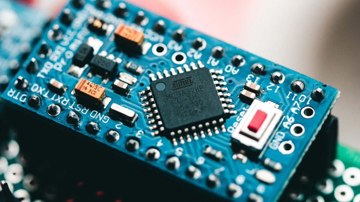
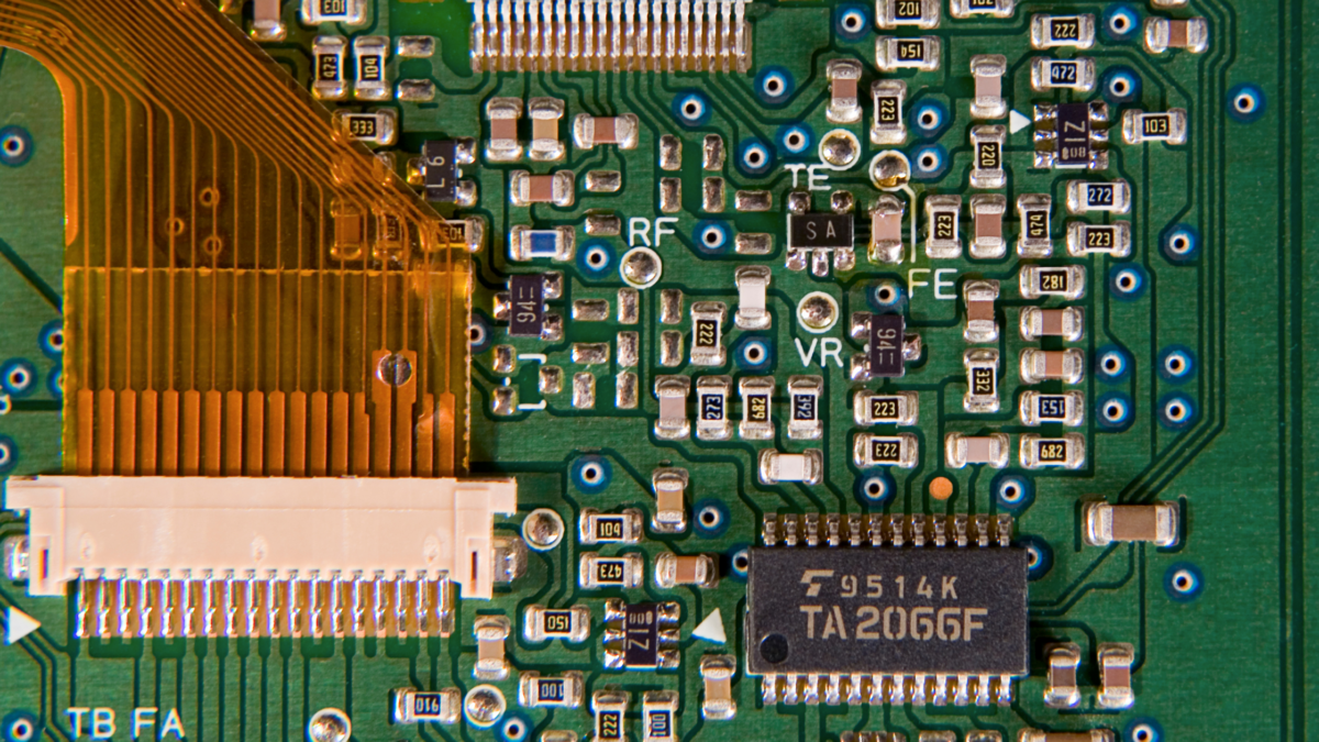
Printed circuit boards are used in practically anything electronic, including toys for kids, cars, and machinery for industrial manufacture. PCBs are crucial to numerous applications and are made from fibreglass, epoxy, metal components, and a green solder mask.

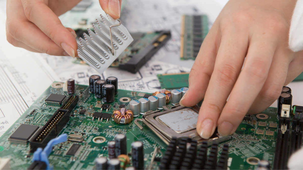
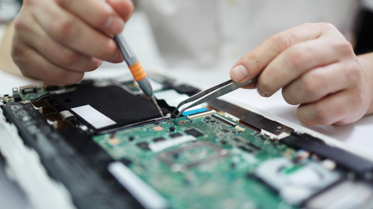
The components are arranged on it to enable the PCB to perform as intended. The PCB’s functionality is what matters most. Even if a tiny SMT resistor is not installed correctly or a little track is removed from the PCB maker, the PCB may still not function. Therefore, the parts must be put together correctly. When components are assembled, the PCB is referred to as an “assembled PCB” or “PCBA.” Here are some types of PCB Assembly processes:

Rigid-Flex Printed Circuit Board Assembly

Printed circuit boards, known as rigid-flex boards, combine stiff and flexible board technology. Depending on the application’s architecture, most rigid-flex boards are built from many layers of flexible circuit substrates outwardly or internally connected to one or more rigid boards. The flexible substrates are frequently moulded into the flexed curve during production or installation since they are intended to be flexible at all times.

Mixed Assembly

You cannot assemble various components using SMT technology, although it has replaced other mounting techniques in PCB fabrication. Then, the same board must be used for THT and SMT assembly. A mixed assembly uses various techniques but doesn’t require solder paste in the manufacturing process. Many components need to get welded with a surface mount arrangement on the board, except a few speciality components that are not accessible through the SMT process and must be constructed using mixed PCB.

Through-Hole Assembly

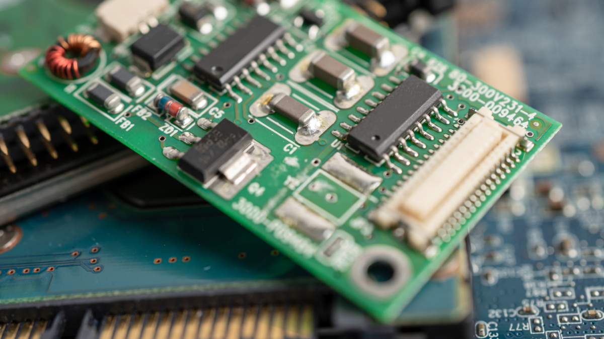
Electronic circuits are constructed utilising the through-hole assembly technique, in which leads are employed to position the components. It describes the assembly procedure, in which the leads are inserted into the pre-drilled holes before the components are joined to the board using either wave soldering or manual soldering. PCB design has historically used multi-layer, double-layer, and single-sided boards. Through-hole assembly is challenging to adapt to the needs of contemporary electronics.

Today, SMT technology has largely taken the place of through-hole assembly in the production of PCBs. However, some applications, such as those utilising electrolytic capacitors, connections, and substantial transformers, still call for through-hole installation.

BGA Assembly

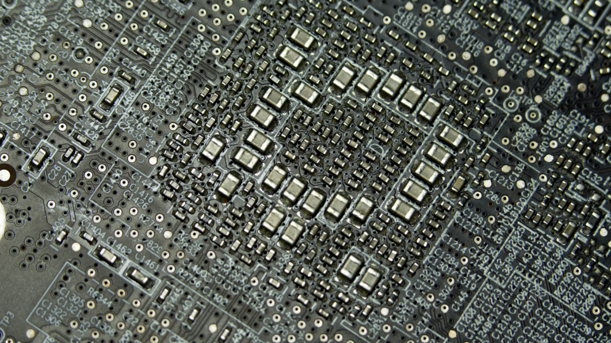
Surface-mount devices called ball grid arrays (BGA), also called chip carriers, are used for packaging integrated circuits. Microprocessors are installed permanently via BGA packaging. A BGA can accommodate more connector pins than a dual in-line or flat design. Instead of merely using the edge, the device’s entire bottom surface can be used. A perimeter-only type frequently has shorter traces than another, which improves performance at high speeds. These traces connect the package’s leads to the balls or wire and connect the package and the die.

SMT Assembly

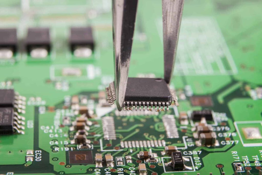
Surface Mount Technology, or SMT, is the official name. SMT is a technique for attaching parts or components to circuit boards. SMT’s superior results and enhanced effectiveness have compelled the replacement of traditional PCB assembly methods. In the past, through-hole assembly was mostly used by PCB manufacturers to add components. However, welding technology has replaced the previous assembling technique in SMT.

All electronic businesses, including those in computers, phones, smartphones, home appliances, etc., employ PCBs made using the SMT assembly technique. Printing solder paste, mounting components, reflow soldering, and carrying out AOI or AXI are the basic procedures in SMT assembly.

Conclusion

Most PCBs that deliver high voltage or current have a separate plane for ground connections. The top layer’s electronic components are “Vias” connecting to the inner GND plane or signals layer. You can use any of the above processes, but ensure to have the right equipment.

Top 5 Latest Equipment You Need for Assembling Your Boards

While making PCBAs is a fun task, learning how the brains of all electronics are created offers joy and a sense of accomplishment. Each step of the assembling process is carefully thought out to produce a board that works flawlessly. Additionally, as electronics become more sophisticated, PCB manufacturing equipment is increasing and becoming more fascinating than ever.

Solder Paste Printing Machine

Solder paste is applied to the board as the initial step in PCB assembly. Usually composed of tin, lead, and silver alloys, solder paste is a grey-coloured goo formed from a combination of very microscopic metal particles. Consider it as the glue holding your finished board together. Components wouldn’t adhere to your bare board without it.

The PCB is covered with a stencil before the paste is applied. A PCB stencil is a piece of stainless steel with tiny laser-cut holes that allows solder paste only to be applied to the SMD pads, which are the board parts where the component connections will eventually be located on the finished PCB.

Glue Dispensing Machine

The glue dispensing machine uses glue dots on the PCB before component insertion to hold the component bodies until the leads and contacts are connected. This is crucial for reflow soldering or double-sided wave to prevent component drop-off and wave soldering, where the force of the solder wave may remove bigger components.

Reflow Soldering Machine

The most used soldering method for PCB assembly is reflow soldering. The assembly is transported via a conveyor via a lengthy, enormous oven called the reflow soldering machine once the board has been fully populated with components. As the PCB boards move through several temperature-controlled zones, the solder paste melts and steadily hardens to make reliable electrical connections between the component pads and their corresponding components.

The circuit board is moved along a conveyor system through the equipment’s various temperature zones. The solder paste is dried, heated, melted, wetted, and chilled before the components are soldered to the printed circuit board. The main component of reflow soldering is using an external heat source to heat the solder, causing it to melt, flow, and re-infiltrate the circuit board.

Automated Optical Inspection (AOI)

The boards have now been assembled, and testing and inspection are next. Automatic visual inspection is more crucial than ever due to the rise in the complexity of PCB boards. Even though you can still try to use your naked eyes to discover errors, manual inspection is ineffective for mass production since workers quickly become worn out, and errors are more likely to be overlooked. Testing PCBAs is essential in PCBA manufacture to prevent expensive re-manufacturing costs and material waste. AOI systems identify issues early in the production cycle, allowing for the modification of methods or the correction of specific boards.

AOI systems can complete tests formerly done by humans but much more quickly and accurately by using optical technologies to detect errors. The AOI machine uses high-resolution cameras to capture the board’s surface and create an image for analysis.

Functional Validation Test (FVT)

Before shipment, completed PCBs must pass Functional Validation Testing (FVT), which is the last phase. We are no longer merely looking for physical flaws like solder bridges or tombstones. The board is instead loaded with software, and we are testing to see if it will function when utilised in whatever application our customers have in mind.

Conclusion

Likely, components won’t be manually soldered when many PCBs need to be created. Expert assembly companies steps in to assist with the fabrication of both the bare boards and the assembly of all the parts into the Printed Circuit Boards, or PCBs.

Understanding the Role of Surface Mount Technology in Circuit Board Assembly

Also known as SMT, surface mount technology is soldering various parts of the circuit board directly onto the circuit board. It is considered a breakthrough in the PCB industry, mainly due to its benefit of cutting costs without cutting corners on quality.

SMT comes under the electronic component assembly phase of the circuit board construction, and this technology is designed to be directly mounted onto the actual circuit board.

Let us delve deeper into this technology, understanding what SMT is in greater detail and looking at the manufacturing process in further detail.


Surface Mount Technology: Explained

This piece of technology is utilized during the assembly of the PCB and is a production method that involves directly embedding various electrical components onto the PCB.

The main selling point and a major reason why this is considered such a beneficial technique for PCB production are that the entire circuit board creation process can now be fully automated

 because of how it works. 

The parts installed onto the PCB are surface-mounted devices or SMD.


How does it work?

What makes SMT an upgrade is that it eliminates the time-consuming process of mounting components onto the board by making holes to insert them in.

Using SMT, you can solder the parts directly onto the PCB using a technique called reflow soldering, shedding a great amount of time that would be spent when assembling the board using the conventional production method.

However, circuit boards made through SMT are usually automated by integrating different machinery into the production process. The overall process can prove to be time-consuming because of the precision required when soldering the parts onto the spots on the board.

Incredibly high precision and accuracy are required when installing the parts into the circuit board through this method, which is why special machinery is developed known as surface mount assembly.

 Applying parts onto the circuit board using SMT is required primarily since this technology involves incredibly small components compared to the components which are fit using the through-hole assembly method.

PCB Manufacturing Process using SMT

1. Prepping the Board and Necessary Components

Before soldering any component onto the circuit board, performing certain tasks to prepare them is usually handled during the board, component, and board design stage.

The initial state of the PCB comprises a board that comprises a copper or gold pad, also known as a solder pad.

Stencils are a vital tool used during manufacturing to provide each component with a set position, which is necessary for the paste printing process.

2. Solder Paste Printing

This is a vital phase of the SMT manufacturing process, where a special printer applies paste onto the predetermined positions set using the stencil. Ensuring the paste is applied to the correct positions is vital because it holds the mounted components in place.

3. Applying the Components

After solder paste has been applied to the different spots and the board has been prepared, it is time for the components to fit onto the board using SMT.

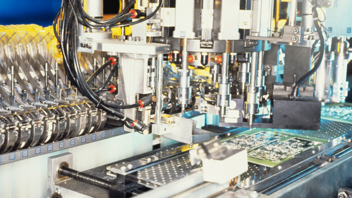
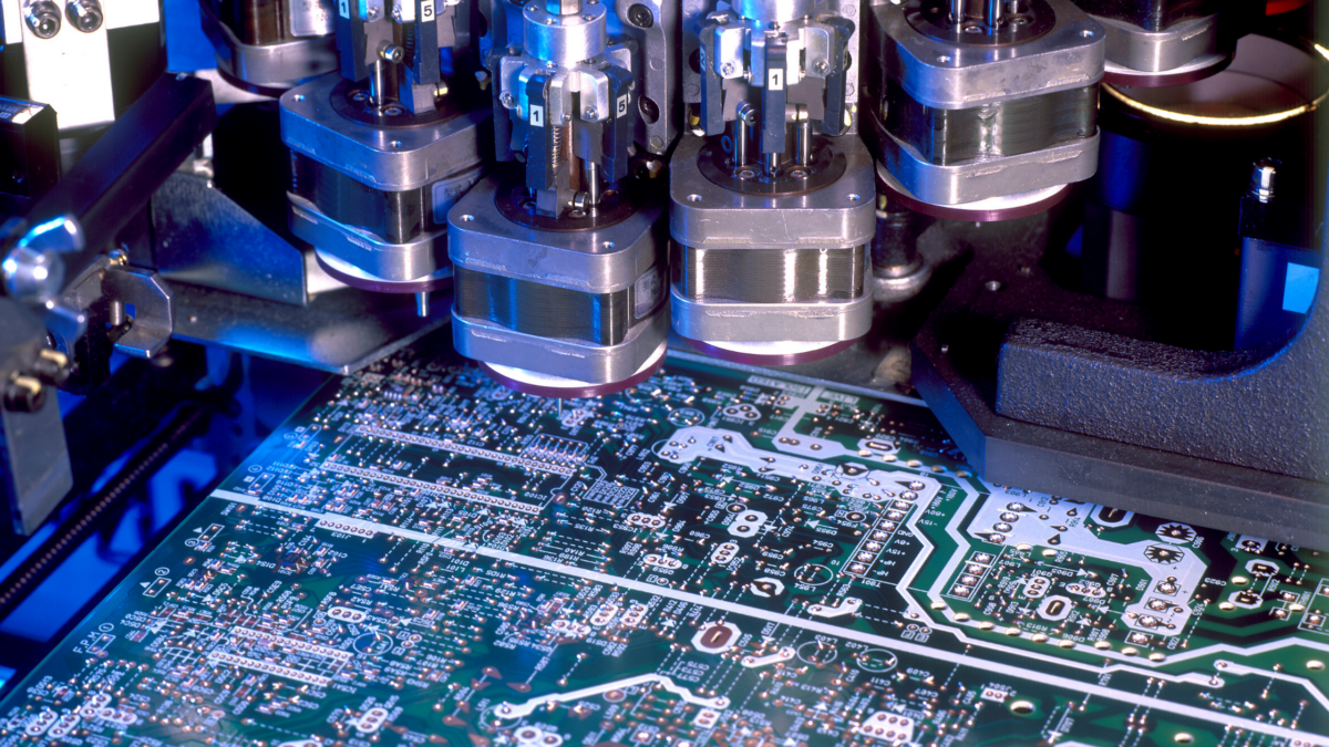
Special machinery ensures that the devices are mounted precisely onto the position assigned to each of them. Since the boards are moving on a conveyer belt, with each machine working by applying a part on the board while the PCB moves, accuracy is vital.

4. The Reflow Soldering Process

Once the SMCs have been installed onto the circuit board, the conveyer belt takes the PCB through the soldering oven comprising different zones. This soldering method is designed to accelerate the setting and drying process to ensure that the solder has been applied and the components have been set in place as soon as possible.

5. Thorough Inspection

After the PCB has been fully assembled, it goes through cleaning, and a final inspection is made to check for possible flaws or defects that might occur during the assembly.


Conclusion

Judging by the information above, surface mount technology has successfully automated the entire PCB production and manufacturing process, which is mainly why it is considered such a breakthrough in PCB assembly.


The Environmental Impact of Circuit Board Assembly

Environmental concerns are at the forefront of discussions in almost every industry, including electronics manufacturing. Circuit board assembly, a fundamental process in electronics production, has a significant environmental impact. This impact encompasses various stages of the assembly process, from material selection and presentation to waste management. In this article, we will delve into the environmental consequences of circuit board assembly and explore strategies to mitigate its impact.

Material Selection and Sourcing

The environmental footprint of circuit board assembly begins with selecting and sourcing materials. PCBs consist of various components, including substrates, copper, solder, and electronic components. These materials often have complex supply chains that can be environmentally taxing.

  • Substrates

Traditional PCB substrates like FR-4 are based on fiberglass-reinforced epoxy resins. While widely used, the production of epoxy resins involves hazardous chemicals. Manufacturers are increasingly exploring alternative substrate materials like biodegradable or recyclable options to reduce environmental impact.

  • Copper

Copper is a primary conductor in PCBs, and its production requires significant energy and can generate emissions. Recycling copper is an eco-friendly option that reduces the need for mining and processing of virgin copper.

  • Solder

Lead-based solders have been phased out due to their environmental and health hazards. The shift to lead-free solders has improved the environmental profile of solder materials. However, lead-free solders may still contain other potentially harmful elements, making proper disposal and recycling crucial.

Energy Consumption

The manufacturing process of circuit boards consumes substantial energy. The operation of manufacturing equipment, especially for surface mount technology (SMT) assembly, involves high-temperature reflow soldering ovens and other power-intensive processes. Reducing energy consumption through more energy-efficient machinery and practices can help mitigate this impact.

Emissions and Air Quality

Soldering and other assembly processes can release volatile organic compounds (VOCs) and other pollutants into the air. Proper ventilation and emissions control equipment are essential to minimize these emissions. Transitioning to lead-free soldering has also reduced the emission of harmful substances like lead into the atmosphere.

Waste Generation

Waste generation is a significant environmental concern in circuit board assembly. This waste includes off-cuts of substrate material, defective PCBs, trimmings from component leads, and obsolete or end-of-life electronic components. To address this issue:

  • Recycling

Recycling PCBs and electronic components can recover valuable materials like copper and precious metals while reducing the need for resource-intensive extraction.

  • E-Waste Management

Proper disposal of electronic waste (e-waste) is crucial. Many countries have regulations and programs for the safe recycling and disposal of electronic products to prevent hazardous materials from entering landfills.

Chemical Usage and Pollution

The use of chemicals in circuit board assembly, such as fluxes and cleaning agents, can have environmental implications. Some of these chemicals may be hazardous if improperly handled and disposed of. Adopting eco-friendly fluxes and cleaning agents less harmful to the environment and human health can help mitigate this impact.

Transportation and Logistics

The transportation of materials and finished circuit boards also contributes to the environmental footprint. Efficient logistics management and the use of low-emission transportation options, such as electric vehicles or those powered by renewable energy sources, can help reduce the carbon footprint associated with circuit board assembly.

End-of-Life Considerations

The environmental impact of circuit board assembly extends beyond the manufacturing stage. Proper disposal or recycling is essential when electronic products reach the end of their life cycle. E-waste recycling programs and initiatives ensure that electronic components and PCBs are safely and sustainably managed.

Mitigating the Environmental Impact

To reduce the environmental impact of circuit board assembly, several strategies can be employed:

  • Design for Sustainability

Engineers and designers can incorporate sustainability principles into the PCB design. This includes selecting eco-friendly materials, minimizing energy consumption, and designing for easy disassembly and recycling.

  • Supplier Collaboration

Collaborating with environmentally responsible suppliers can help ensure that materials are sourced sustainably, and environmentally friendly production methods are employed.

  • Regulatory Compliance

Staying compliant with environmental regulations and standards is essential. Many countries have stringent regulations governing the use and disposal of hazardous materials in electronics manufacturing.

  • Recycling and Reuse

Implement recycling programs for PCBs and electronic components. Encourage the recycling and repurposing of old electronics whenever possible.

  • Energy Efficiency

Invest in energy-efficient equipment and manufacturing processes to reduce energy consumption.

  • Waste Reduction

Implement waste reduction strategies, such as optimizing material usage and minimizing scrap.

Conclusion

The environmental impact of circuit board assembly is a multifaceted issue that spans material sourcing, manufacturing processes, waste management, and end-of-life considerations. Mitigating this impact requires a holistic approach that includes sustainable material selection, energy-efficient manufacturing, responsible waste management, and adherence to environmental regulations.

By embracing environmentally friendly practices and promoting sustainability at every stage of circuit board assembly, the electronics industry can reduce its ecological footprint and contribute to a more sustainable future.

The Role of PCBs in IoT Devices: Challenges and Solutions

[et_pb_section fb_built=”1″ admin_label=”section” _builder_version=”4.16″ global_colors_info=”{}”][et_pb_row admin_label=”row” _builder_version=”4.16″ background_size=”initial” background_position=”top_left” background_repeat=”repeat” global_colors_info=”{}”][et_pb_column type=”4_4″ _builder_version=”4.16″ custom_padding=”|||” global_colors_info=”{}” custom_padding__hover=”|||”][et_pb_text admin_label=”Text” _builder_version=”4.24.2″ background_size=”initial” background_position=”top_left” background_repeat=”repeat” hover_enabled=”0″ global_colors_info=”{}” sticky_enabled=”0″]

For the IoT industry, PCBs are the unsung heroes who create functional connections in IoT devices. As the building block of electronic devices, PCBs play an important role in fostering IoT technologies’ efficiency, performance, and reliability. This thin board is made of insulating material with conductive copper track, allowing electronic components to route their connectivity for a circuit.

However, this building block comes with its own set of challenges that we will address so that you can see why your IoT device is acting up. Although these challenges can be a huge hindrance for us, they come with their solutions and an opportunity for us to learn and grow.

Challenges Faced by PCBs in IoT Devices

As IoT aims to connect and network devices, it is on OCB designs to mold how they work.

Size Constraints and Miniaturization

Printed circuit boards (PCBs) face a formidable challenge in IoT due to the devices’ ever-shrinking size requirements. As IoT applications demand increasingly compact and portable solutions, PCBs must grapple with the intricacies of miniaturization. This section explores the impact of size constraints on PCB design, examining the trade-offs between functionality and space efficiency. Strategies such as multi-layered PCBs and surface mount technology will be discussed to address the miniaturization challenge in IoT devices.

Power Consumption Issues

Efficient power management is critical in IoT devices where prolonged battery life and energy conservation are paramount. PCBs face the challenge of optimizing power distribution, minimizing energy loss, and ensuring overall energy efficiency. This segment delves into the intricacies of power consumption challenges, exploring how advanced power delivery systems, low-power components, and intelligent design can mitigate power constraints’ impact on PCBs in IoT applications.

Environmental Factors and Durability

IoT devices often operate in diverse and demanding environments, ranging from extreme temperatures to high humidity or corrosive conditions. PCBs must contend with maintaining functionality and structural integrity under such varied circumstances. This section explores the impact of environmental factors on PCB performance, delving into materials engineering, protective coatings, and design considerations that enhance the durability of PCBs in IoT devices.

Solutions to PCB Challenges in IoT Devices

With these solutions, it is prominent that IoT devices are revolutionizing PCBs’ basic structure and design.

Advanced Manufacturing Techniques

The implementation of advanced manufacturing techniques becomes crucial to address the challenges posed by size constraints and the need for miniaturization in PCBs for IoT devices. This section explores cutting-edge methods such as additive manufacturing, HDI (High-Density Interconnect) technology, and precision assembly processes. By adopting these approaches, engineers can optimize space utilization, enhance component integration, and overcome the limitations associated with the physical dimensions of IoT devices.

Energy-Efficient Design Strategies

Efficient power consumption is a cornerstone in the successful operation of IoT devices. PCBs play a pivotal role in achieving energy efficiency. This segment delves into design strategies that minimize power consumption without compromising performance. Topics include utilizing low-power components, smart power management systems, and implementing energy harvesting technologies. IoT devices can extend battery life and reduce their environmental impact by adopting these energy-efficient design principles.

Materials Innovation for Durability

PCBs must be robustly durable to ensure the longevity of IoT devices. This section explores innovative materials and coating technologies that enhance PCB resilience. A detailed examination of material science solutions will be provided, from corrosion-resistant materials to protective coatings that shield against harsh environmental conditions. By integrating these advancements, PCBs can withstand the rigors of varied environments, ensuring the reliability and durability of IoT devices.

As we delve into these solutions, it becomes evident that the evolution of PCB technology is intricately linked to overcoming the challenges posed by IoT requirements. Integrating advanced manufacturing techniques, energy-efficient designs, and innovative materials is paving the way for more resilient and high-performing PCBs in the rapidly expanding landscape of Internet of Things applications.

Wrapping Up

As we go through these challenges and their recurring solutions, we tend to address the designers’ perspective and also what IoT industries face. On the other hand, this era of innovation demands more user-friendly PCBs so that they can easily be integrated into the devices.

[/et_pb_text][/et_pb_column][/et_pb_row][/et_pb_section]

Printed Circuit Board Assembly (PCBA) Process- A Comprehensive Guide

Have you ever wondered about the structure of electrons that brings your electronic devices to life? Modern electronics have the printed circuit board assembly (PCBA) process that orchestrates this structure, transforming raw components into functional devices. Every electronic device we encounter is connected to the PCB in some way. Everything from smartphones, cars, home appliances, computers, etc., has these electronic building blocks.

Deepening technological advancements and evolving with time, the PCBA process transforms a design into a fully operational circuit. Although it may seem daunting at first, it is quite easy. Before that, you must know about the components used in PCBA.

The Basic Components Of PCB

The PCBA components are essential building blocks that transform a blank circuit board into a functional electronic device. Understanding these components is crucial for anyone delving into the intricate world of Printed Circuit Board Assembly (PCBA). When carefully orchestrated, these elements breathe life into the electronic devices that have become integral parts of our daily lives. Here we tell you about the key elements:

  • Integrated Circuits (ICs)
  • Resistors
  • Capacitors
  • Inductors
  • Diodes
  • Transistors
  • Connectors
  • Resonators and Oscillators
  • Microcontrollers
  • Sensors

The PCBA Process Steps

Step 1. Design and Layout

The Design and Layout phase of the Printed Circuit Board Assembly (PCBA) process is the foundational stage where the blueprint of the circuit board comes to life. Designers utilize specialized software, typically CAD (Computer-Aided Design), to meticulously plan the placement of components, signal traces, and layers. This step is pivotal in ensuring optimal functionality, as a well-thought-out design directly impacts the efficiency and manufacturability of the PCB. Designers must carefully consider factors like signal integrity, thermal management, and electromagnetic interference, laying the groundwork for the subsequent stages of the PCBA process.

Step 2: Fabrication of PCB

Fabricating a PCB involves transforming the design into a tangible board. This step includes selecting appropriate substrate materials, commonly fiberglass reinforced with epoxy and copper foils for the conductive layers. The fabrication process employs techniques like etching, layering, and coating to create the final PCB. The precision and quality of fabrication significantly influence the overall performance and reliability of the electronic device.

Step 3: Component Placement

Determining how components will be placed on the PCB is critical in the PCBA process. Engineers must choose between automated assembly machines or manual labor for precise component placement. This step’s precision is crucial as it directly affects the final electronic device’s functionality and efficiency. Careful consideration is given to optimizing the use of space on the PCB.

Step 4. Soldering

Soldering is the process that brings the PCB to life by creating electrical connections between components and the board itself. There are two primary techniques: Surface Mount Technology (SMT), where components are mounted directly onto the PCB surface, and Through-Hole Technology (THT), where components are inserted into drilled holes on the PCB. Reflow soldering, a common method, involves melting solder to form secure connections. The success of the soldering step ensures the reliability of the entire PCBA.

Step 5: Inspection and Testing

After assembly, thorough inspection and testing are crucial to guarantee the quality and functionality of the PCB. Visual inspection, automated optical inspection (AOI), and X-ray testing are common quality control measures. Functional testing ensures that the assembled PCB meets performance specifications, identifying and rectifying any defects before the final product reaches the end-user.

Step 6: PCB Design Considerations

PCB Design Considerations encompass the principles and guidelines that govern the layout, trace routing, and component placement during the design phase. These considerations are essential for achieving optimal performance, signal integrity, and reliability in the final product. Factors influencing design include the type of electronic components, the intended application, and the overall goals of the electronic device.

Step 7: Fabrication of PCB

Fabricating a PCB involves transforming the design into a tangible board. This step includes selecting appropriate substrate materials, commonly fiberglass reinforced with epoxy and copper foils for the conductive layers. The fabrication process employs techniques like etching, layering, and coating to create the final PCB. The precision and quality of fabrication significantly influence the overall performance and reliability of the electronic device.

Step 8: Component Placement

Determining how components will be placed on the PCB is critical in the PCBA process. Engineers must choose between automated assembly machines or manual labor for precise component placement. The precision of this step is crucial as it directly affects the functionality and efficiency of the final electronic device. Careful consideration is given to optimizing the use of space on the PCB.

Step 9: Soldering Techniques

Soldering techniques are integral to the PCBA process, determining how components are securely connected to the PCB. Surface mount technology (SMT) involves mounting components directly onto the PCB surface, while through-hole technology (THT) involves inserting components into drilled holes on the PCB. Reflow soldering, a widely used technique, melts solder to form reliable connections, ensuring the electronic device’s durability and performance.

Step 10: Inspection and Testing

Inspection and Testing are critical steps to verify the quality and functionality of the assembled PCB. Various quality control measures are employed, including visual inspection, automated optical inspection (AOI), and X-ray testing. Functional testing ensures that the PCB meets specified performance criteria, identifying and rectifying any defects before the final product reaches the end-user.

The PCBA process is a multifaceted journey from design to a fully operational circuit. Each step plays a role in ensuring the final electronic device’s functionality, reliability, and performance. As technology advances, the PCBA process evolves, presenting new opportunities and challenges for electronic manufacturers.

Common PCB Manufacturing Challenges and Their Solutions

The printed circuit board, PCB, bridges the gap between signals and powers. It makes sure power is directed within electronic devices. These fundamental components are often overlooked in sleek devices. Power is the backbone of connectivity and functionality. However, designing a PCB and making it fully functional can sometimes leave loopholes. These loopholes generate challenges that are caused during the manufacturing phase but show their failure during assembly.

The entire manufacturing of PCBs is riddled with challenges, including the delicate placement of minuscule components, the strategic management of heat, and the selection of materials resilient to diverse environmental factors. But with every challenge comes the solution, and if we fail to find it, we will jeopardize the performance and efficiency of electronic devices.

8 PCB Manufacturing Challenges And Solutions

While dissecting the routes of these challenges, we have curated a set of solutions from industry experts. Addressing these challenges isn’t just a matter of technical finesse; it is a strategic imperative. The smooth functionality of electronic devices hinges on successfully navigating these hurdles. Read on to learn more about the key challenges and the possible solutions.

Design For Manufacturability DFM

Design for Manufacturability (DFM) is a cornerstone for efficient PCB production. Ensuring that the design is conducive to manufacturing is vital in avoiding bottlenecks and errors. Challenges may arise when intricate designs pose component placement or thermal management difficulties. Solutions involve collaborative efforts between designers and manufacturers, incorporating DFM principles early in the design phase to optimize efficiency, reduce costs, and enhance overall manufacturability.

Solder Quality Control

The integrity of solder joints is paramount for the reliability of a PCB. Maintaining consistent solder quality can be challenging, leading to poor connections and premature component failure. Implementing rigorous quality control measures, including visual inspections and automated testing, is essential. Utilizing advanced soldering technologies and adhering to industry standards further ensures the production of PCBs with robust and reliable solder joints.

Slivers

Slivers, minute slivers of copper or other materials between traces, pose a challenge in PCB manufacturing, potentially causing short circuits or signal interference. Precision and thorough inspection are critical to identifying and eliminating slivers. Latest atest manufacturing methodsmethods , such as laser cutting and high-precision etching, help minimize the occurrence of slivers and ensure the integrity of the PCB design.

Missing Solder Masks

The absence of solder masks can result in bridging between solder joints, compromising the PCB’s functionality. Detecting and rectifying missing solder masks requires meticulous inspection and adherence to quality control protocols. Automated inspection systems and the careful application of solder masks during manufacturing are pivotal in preventing and addressing this challenge.

Acid Traps

Acid traps, where etching solutions can become trapped during manufacturing, threaten the
PCB’s integrity. This challenge can lead to uneven copper traces or other structural issues. Implementing effective rinsing and quality control processes in the manufacturing line helps mitigate acid traps, ensuring a clean and uniform etching process.

Material Defects

Material defects, such as inconsistencies in substrate materials, can compromise a PCB’s overall performance and reliability. Thorough material testing and quality assurance procedures are essential to identify and address these defects. Collaborating with reputable material suppliers and maintaining stringent quality control measures in the manufacturing facility are key strategies for minimizing material-related challenges.

BGA Spacing

Ball Grid Array (BGA) components present a specific challenge in PCB manufacturing due to their densely packed nature. Inadequate spacing can lead to issues during soldering and compromise the reliability of the connections. Precision in BGA component placement, utilizing advanced soldering techniques, and implementing thorough inspection processes are crucial for overcoming spacing challenges and ensuring the integrity of BGA connections.

Test Point Existence

Test points are essential for diagnosing and troubleshooting PCBs during and after manufacturing. The challenge is ensuring that these test points exist and are accessible. Incorporating standardized test point designs, strategically placing them on the PCB, and employing automated testing procedures contribute to overcoming this challenge, facilitating efficient testing and quality assurance throughout the manufacturing lifecycle.

Conclusion

There you go! By understanding the intricacies of PCB manufacturing challenges and proactively seeking solutions, manufacturers can ensure the reliability and quality of their products and position themselves at the forefront of technological advancement.

Advancements in Materials – Explore Latest in PCB Substrates

While traditional materials have served as the backbone of PCBs, a closer examination reveals inherent limitations and challenges. Understanding these constraints sets the stage for exploring cutting-edge solutions. The heart of innovation lies in printed circuit boards (PCBs) for the electronics industry. Within this dynamic industry, the substrates that underpin PCBs have emerged as a focal point of exploration and advancement. PCB substrates have moved from the foundations of traditional materials to the noncomposite wonders. By discussing how these advancements are reshaping industries and propelling us into an era of unprecedented electronic possibilities, we will know how to take leverage of this advancement.

What Are PCB Substrates?

Printed Circuit Board (PCB) substrates are the foundational materials that provide mechanical support and electrical insulation for the components on a PCB. These substrates serve as the base upon which the conductive paths and electronic components are mounted. Typically composed of insulating materials, PCB substrates play a crucial role in supporting the conductive traces that facilitate the flow of electrical signals throughout the circuit.

The choice of substrate material is vital, influencing the board’s performance, reliability, and overall functionality. Common materials used for PCB substrates include fiberglass-reinforced epoxy laminates (FR-4), which are widely employed in conventional PCBs, and more advanced materials like flexible polymers or ceramics for applications requiring flexibility or high-frequency performance.

Latest Innovations in PCB Substrates

PCB substrates provide a platform for the intricate interconnection of electronic components, enabling the creation of complex circuits that power a diverse array of electronic devices, from smartphones to industrial machinery. The continual innovation in PCB substrate materials contributes to the ongoing evolution of electronic technology, allowing for improvements in performance, miniaturization, and the development of new functionalities.

High-Frequency Materials

High-frequency materials represent a significant stride in the evolution of PCB substrates, particularly in response to the demands of new tech such as 5G communication. These materials exhibit low signal loss and enhanced signal integrity, crucial for transmitting data at higher frequencies. Common high-frequency substrate materials include polytetrafluoroethylene (PTFE) and ceramic-filled hydrocarbons. Adopting these materials enables the design of PCBs capable of supporting the rapid data rates required for next-generation wireless communication and other high-frequency applications.

Flexible and Rigid-Flex Substrates

The advent of flexible and rigid-flex substrates marks a departure from the rigid confines of traditional PCBs. Flexible substrates, often composed of polyimide, allow PCBs to bend or conform to non-planar surfaces, opening up new possibilities for wearable devices and unconventional form factors. Rigid-flex substrates combine flexible and rigid materials in a single board, balancing adaptability and structural integrity. This innovation is reshaping the design landscape, enabling the creation of foldable smartphones, flexible displays, and other compact electronic devices.

Nanocomposite Materials

Nanocomposite materials revolutionize PCB substrates by incorporating nanoparticles into the base material. These nanoparticles, often carbon-based, enhance mechanical strength, thermal conductivity, and electrical properties. The resulting PCBs exhibit improved performance, reduced size, and increased reliability. Nanocomposites are especially valuable in applications where size and weight are key factors, such as aerospace and medical devices. As technology advances, integrating nanocomposite materials into PCB substrates propels electronic devices into realms of previously unimaginable efficiency and capability.

Final Thoughts

Exploring the latest innovations in PCB substrates reveals a tapestry of technological breakthroughs poised to redefine electronic devices’ capabilities and design possibilities. The convergence of high-frequency precision, flexible adaptability, and microscopic enhancements of nanocomposite materials underscores the dynamic nature of electronic engineering. It sets the stage for a future where devices are interconnected and optimized for efficiency, performance, and versatility.

As we stand on the brink of this transformative era, the journey through these innovations in PCB substrates signals progress and a profound leap forward into the next generation of electronic design and functionality.

A Beginner’s Guide to Circuit Board Assembly

You may not realize it, but printed circuit boards are more important and common than you think. Present within a vast majority of the electronic devices we use daily, these circuit boards are a vital component that ensures the proper functionality of electronics.

Keeping this in mind, it is essential to understand that the assembly of these circuit boards is vital, primarily because they are a major component within electronics.

Because of the components and circuitry involved within an average PCB, the manufacturing process is incredibly complex.

Not only that, but the board you are working on also needs to be reliable enough to support the assembly process so that the resulting PCB does not turn out to be faulty.

Let us discuss this in further detail, exploring deeper into the concept of PCB assembly, understanding the resources needed, and the assembly process itself.

PCB Assembly: In Depth

Before going into the specifics of the overall process, let us first establish a foundation: the assembly process, taking a broader look at this part of PCB development.

Simply speaking, the initial state of a circuit board that has yet to go through any component installation is a printed circuit board, also known as the PCB.

When the necessary electrical components have been installed onto the board, the resulting circuit board that we end up with is called the printed circuit board assembly, otherwise known as a PCBA.

Many people consider the PCB assembly and manufacturing process as the same thing, but that is not the case.

The main reason why assembling the circuit board is different is that when the PCB is being manufactured, it goes through a selection of different catering to the design and creation of the board.

However, assembly is what comes after the board has been developed after going through the design phase, involving the assembly of the electronic parts according to the main function of the PCB.

Resources Needed for PCB Assembly

Some certain tools and components are required to ensure that the overall assembling of the PCOB goes smoothly, and these include:

  • The printed circuit board itself
  • Transistors and other basic electronic components
  • A soldering flux
  • Necessary tools to perform a solder, including a soldering wire, soldering iron, and testing equipment.

Different Techniques of PCB Assembly

Even though the through-hole insertion technique for applying electrical components was the only way to develop PCBs, technological advancements have led to other methods, such as assembling a circuit board through SMT.

Assembling Using Thru-Hole Components

This type of PCB assembly involves certain components with wiring coming out of them, which go through the tiny holes within the PCB and are soldered.

When assembling a PCB using thru-hole components, it goes through a process called wave soldering, which involves the being applied in the form of a solder bar, which is put in an incredibly hot bath. This high temperature makes the solder stay molten and creates a wave-like design.

Once the wave has been made, the electrical components are passed through the molten state to be fitted within their places.

The overall assembling and solder process for these components includes:

  • Insertion of the necessary electronics
  • Applying the solder flux
  • Preheating the solder bar
  • Creating the wave solder
  • Cleaning and inspecting the PCBA
  • Testing the final product

Assembly Using SMT

Also known as surface mounting technology, this assembly process involves special components that do not contain any leads and do not need to go through any holes to be soldered.

Using this technology, they are directly soldered onto the PCB and are highly compatible with automation, leading to machinery automating the entire assembly process.

Conclusion

Many factors need to be considered when assembling a printed circuit board. However, with the right tools and components, you will not face any problems if you follow the steps mentioned above to assemble a PCB.

RoHS Compliance and Lead-Free Soldering Techniques

One of the significant steps towards achieving environmental responsibility was the introduction of RoHS compliance regulations. RoHS, which stands for Restriction of Hazardous Substances, is a directive aimed at reducing the use of hazardous materials in electrical and electronic equipment. This directive has driven the adoption of lead-free soldering techniques in electronics manufacturing. In this article, we will explore RoHS compliance, its significance, and the lead-free soldering methods that have become central to it.

RoHS Compliance: A Brief Overview

The RoHS directive, formally known as Directive 2011/65/EU, originated in the European Union but has had a global impact on the electronics industry. Its primary objective is to restrict the use of specific hazardous substances in electronic and electrical equipment. These substances include:

  • Lead (Pb)
  • Mercury (Hg)
  • Cadmium (Cd)
  • Polybrominated biphenyls (PBB)
  • Hexavalent chromium (Cr6+)
  • Polybrominated diphenyl ethers (PBDE)

The RoHS directive applies to a wide range of electronic products, from household appliances to industrial machinery. Manufacturers and suppliers must comply with RoHS regulations to market their products in the EU and other regions that have adopted similar standards.

The Significance of RoHS Compliance

RoHS compliance carries several significant advantages and benefits, both for the environment and for consumers:

  • Environmental Impact

By restricting hazardous substances, RoHS helps reduce the environmental footprint of electronics manufacturing. It limits the release of toxic materials into the environment, thereby mitigating potential harm to ecosystems and human health.

  • Product Safety

RoHS compliance ensures that electronic products are safer for consumers. It reduces the risk of exposure to hazardous substances, particularly in consumer electronics and appliances that may come into direct contact with people.

  • Recycling and Disposal

RoHS-compliant products are easier to recycle and dispose of responsibly. They contain fewer hazardous materials, making them safer for recycling and preventing the contamination of landfills.

  • Global Market Access

Compliance with RoHS regulations enables manufacturers to access global markets. Many countries and regions outside the EU have adopted similar standards, making RoHS compliance essential for international trade.

Lead-Free Soldering Techniques

One of the most significant changes driven by RoHS compliance is the shift from lead-based solder to lead-free solder in electronics manufacturing. Lead-free soldering techniques have become central to achieving RoHS compliance. Here are key aspects of lead-free soldering:

1. Composition

Lead-free solder alloys are typically composed of various metals, with tin (Sn) being the primary component. Common alloys include Sn-Ag-Cu (SAC), Sn-Cu, and Sn-Ag. These alloys offer comparable or even superior mechanical and electrical properties to traditional lead-based solder.

2. Soldering Temperature

Lead-free soldering often requires higher temperatures than lead-based soldering. This can necessitate adjustments in soldering equipment, such as reflow ovens and soldering irons, to accommodate the higher melting points of lead-free alloys.

3. Compatibility

When transitioning to lead-free soldering, it’s essential to ensure that all components and materials used in the assembly process are compatible with lead-free solder. Some components may require adjustments or alternative materials.

4. Solder Paste and Flux

Lead-free solder paste and flux materials are formulated to work with lead-free solder alloys. These materials play a crucial role in ensuring proper wetting and bonding during the soldering process.

5. Process Control

Control over the soldering process is vital to achieve consistent and reliable solder joints. Manufacturers must fine-tune their soldering profiles to account for the characteristics of lead-free solder, ensuring proper reflow and minimizing defects.

Benefits of Lead-Free Soldering

The adoption of lead-free soldering techniques offers several benefits beyond RoHS compliance:

  • Environmental Responsibility

Lead-free solder reduces the environmental impact of electronics manufacturing by eliminating a highly toxic substance.

  • Health and Safety

Lead-free solder is safer for both manufacturing personnel and end-users, reducing the risk of lead exposure.

  • Recycling

Lead-free solder makes recycling and disposal of electronic products more environmentally friendly.

  • Global Market Access

Lead-free soldering techniques enable manufacturers to access global markets, ensuring their products comply with various environmental regulations.

  • Mechanical Strength

Lead-free solder alloys often exhibit improved mechanical strength, enhancing the reliability of soldered joints.

Conclusion

RoHS compliance and the adoption of lead-free soldering techniques have transformed the electronics manufacturing industry, promoting environmental responsibility, product safety, and global market access. While the transition to lead-free soldering presents challenges, the long-term benefits in terms of sustainability and safety make it a crucial step towards a more responsible and sustainable electronics industry. As technology continues to advance, ongoing research and development will further enhance lead-free soldering techniques, making them even more efficient and eco-friendly.