
Designing and assembling PCBs is an incredibly valuable skill. Nowadays, it is a process that is easy to learn and implement, as long as you are willing to invest your time in it. Back in the early days, the PCB assembly process was time-consuming. However, today, you have many software programs that allow you to design them and get them delivered to your doorstep.
Nonetheless, any mistake that you make in your design can be very costly to you. This is because your design will dictate the assembly process, along with the functioning of the board. With a nonworkable board, the electronic device will also suffer from malfunctions and errors.
To avoid these errors, you must take certain things into consideration when assembling and designing a PCB board.
Do not be Impatient
A printed circuit board is a piece of technology that has a precise and sophisticated design. Each detail is thought-through and requires careful considerations. This is why you must never be impatient in any of the PCB assembly processes.
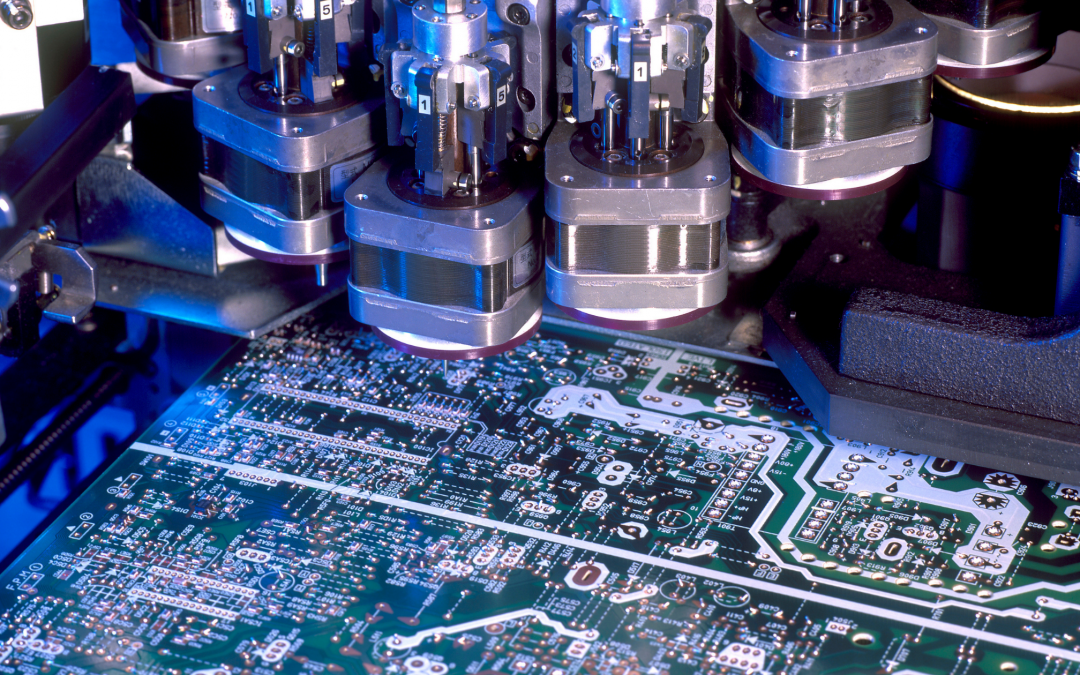
Most people make the mistake of being impatient when they are placing components on the board. According to professional PCB designers, it is integral to have most of the time go to components placement when designing and assembling the PCB.
This is true because the placement framework will ultimately determine the outcome of the PCB design. The trick is to avoid overlapping the rubber panels. Moreover, you have to keep adjusting each placement until there is no overlapping.
When designing, if you spend enough time on your digital component placement, your routing will be significantly easier.
Consider Routing Directions
Once you complete the component placement, then you will have to move forward to routing. For this, you will have to decide the routing direction of a particular layer before laying down the traces.
Make sure that you set the right directions as even the slightest inconsistencies in direction can lead to complete design failure.
Narrow High Current Traces
Make sure that you do not develop the habit of using the same width for all the traces in your design; well, you do not want to do that. Make sure that your traces can withstand the maximum voltage.
If a particular trace carries a higher trace width than the other traces in your design, make sure to increase the width for the others as well. High-width traces ensure proper heat dissipation.
Make use of Copper Pour
Making PCBs involves etching the unused copper and leaving the traces intact. Copper pouring means that you have to use unused copper for any signal instead of etching it out. You have to do it by creating spaces for traces and pads.
Commonly, people will use them for power signals or ground signals. This offers a low impendence path for the current and also makes connection much easier.
Pay Attention to Spacing
Most designers do not consider the importance of spacing and end up making a flawed printed circuit board. Proper spacing requires much more effort and consideration.
Thus, designers should be well aware of the adequate spacing requirements for a particular circuit. You should also consider the assembly of components to ensure proper spacing.
Final Thoughts
These are just a few of the many considerations that you should take when performing a printed circuit board assembly. As you can see, the design process is very important as it can account for an efficient and safe assembly.
Recent Comments