Circuit Board Assembly: How the PCB Assembly Process Works

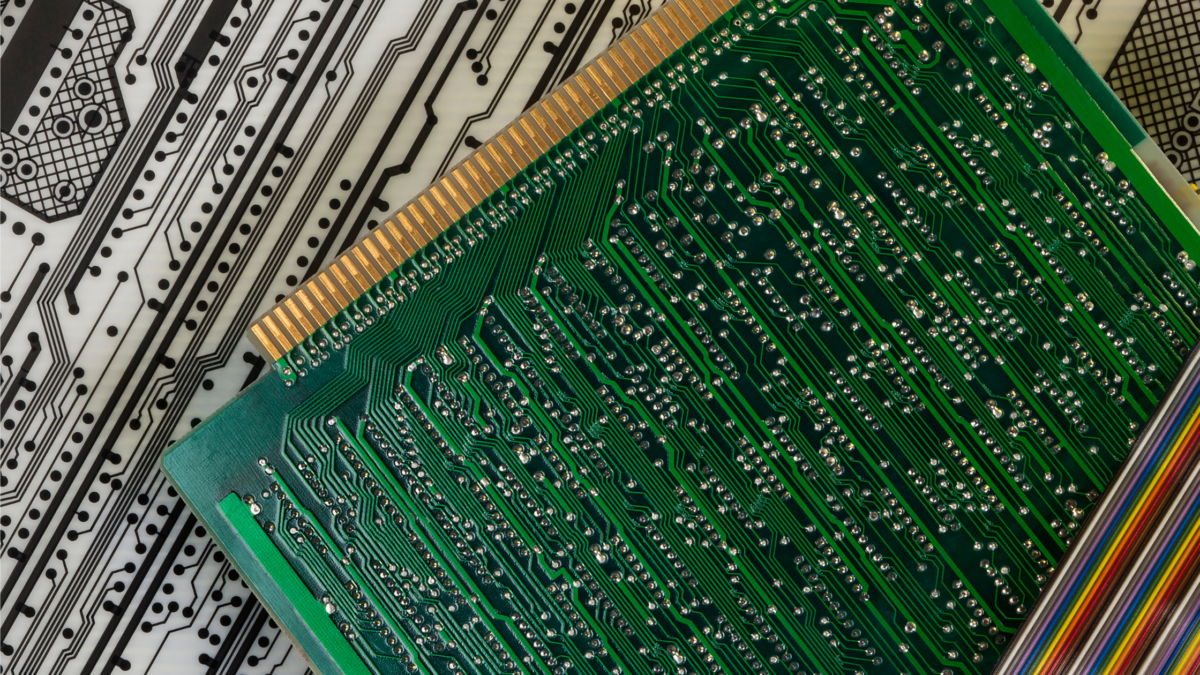
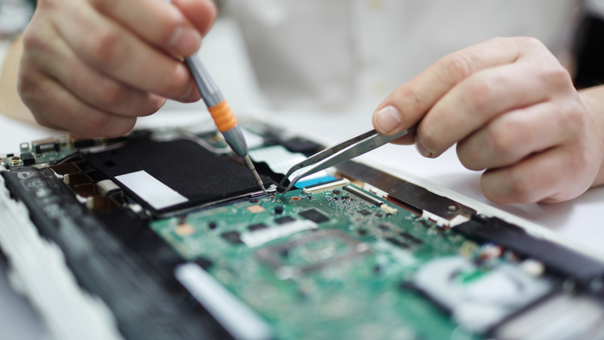
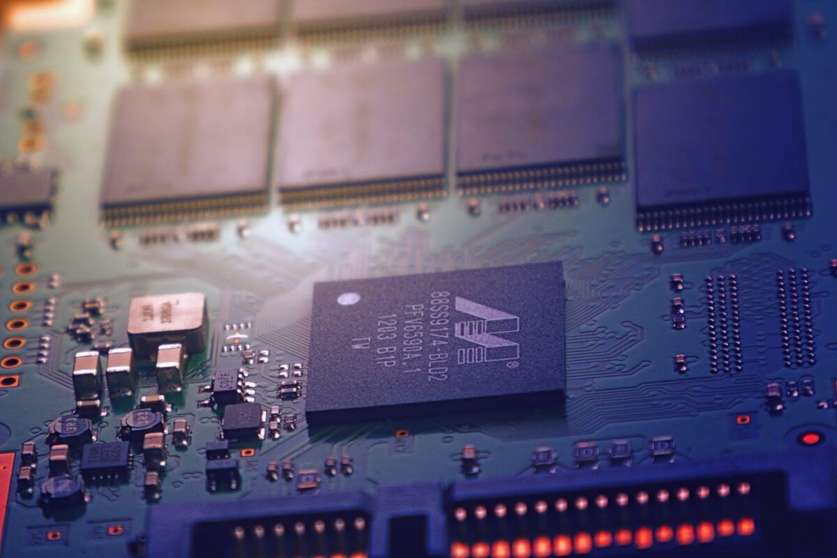
Circuit board assembly is the process that turns a bare printed circuit board into a functional electronic assembly. From medical devices and aerospace systems to industrial equipment and technology, nearly every electronic product depends on accurately assembled circuit boards.
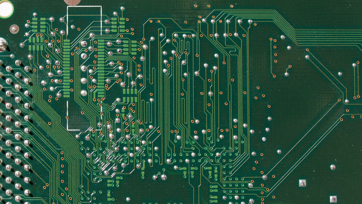
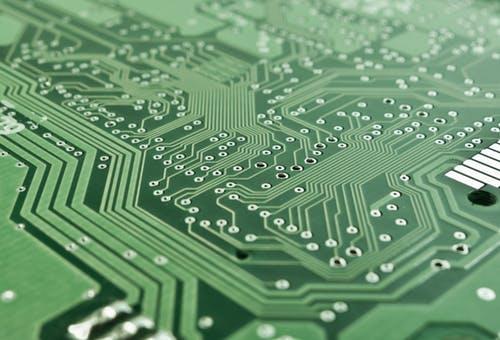
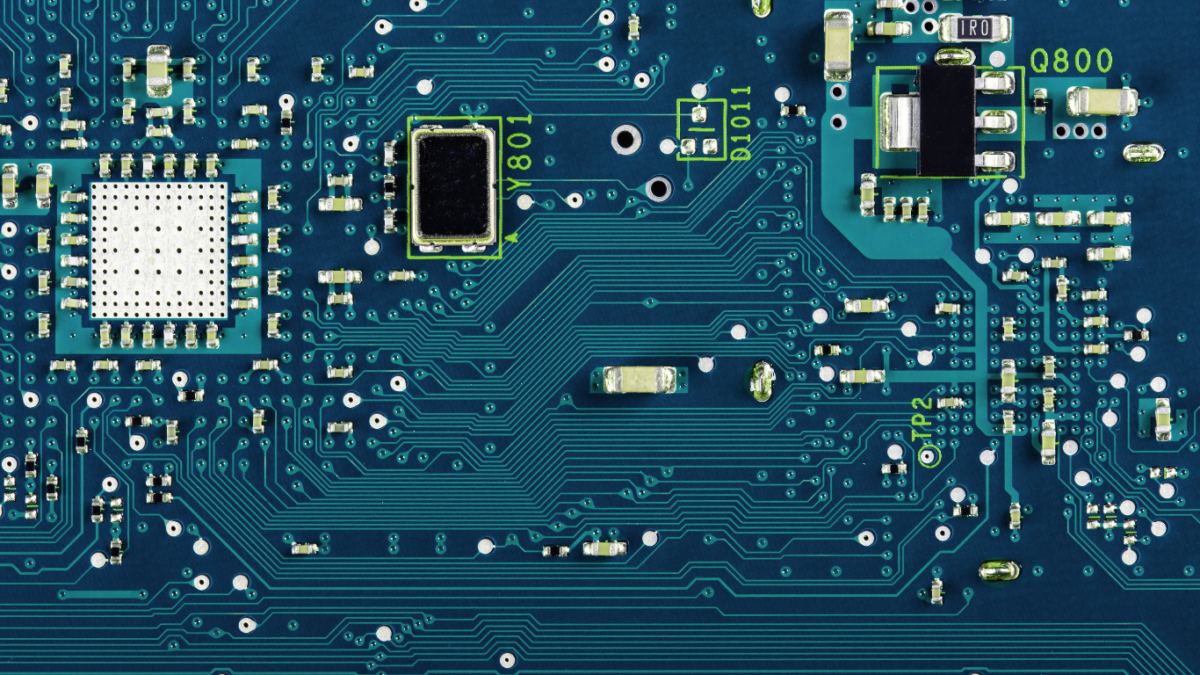
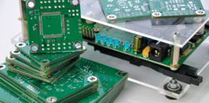
PCB fabrication creates the bare printed circuit board, including its copper traces, layers, holes, solder mask, and other physical features. Circuit board assembly, also called PCB assembly or PCBA, begins when electronic components are mounted and soldered onto that board.
So, what actually happens during the process? Here is a step-by-step look.
1. Design and Manufacturing Review
Successful circuit board assembly starts before a component ever reaches the production line.
Manufacturers review files such as the bill of materials (BOM), Gerber files, placement data, assembly drawings, and special instructions. A Design for Manufacturing, or DFM, review can help identify potential assembly problems before production begins.
This may include checking:
- Component footprints and pad sizes
- Polarity and component orientation
- Solder mask and solder paste alignment
- Component spacing and clearance
- Thermal considerations
- Potential manufacturing or reliability concerns
Finding these issues early can reduce rework, delays, and unexpected problems later in the PCB assembly process.
2. Component Sourcing and Material Preparation
The next step depends on the type of circuit board assembly service being used.
With turnkey PCB assembly, the assembler sources the bare boards and electronic components needed for the project. With consigned assembly, the customer provides the materials. Partial consignment combines the two approaches.
Components must also be properly identified, tracked, and prepared before production begins. Moisture-sensitive materials can require special handling. At Nova Engineering, boards that will pass through the reflow ovens are baked beforehand as part of the preparation process.
3. Solder Paste Application
For surface mount circuit board assembly, solder paste is applied to specific pads on the PCB.
A metal stencil aligns with the board so solder paste is deposited only where surface-mount components will eventually sit. Solder paste contains tiny particles of solder suspended in flux and temporarily helps hold components in position before reflow soldering.
Accurate paste application is important because too much, too little, or poorly aligned solder paste can contribute to solder bridges, weak joints, or other defects.
4. SMT Pick-and-Place
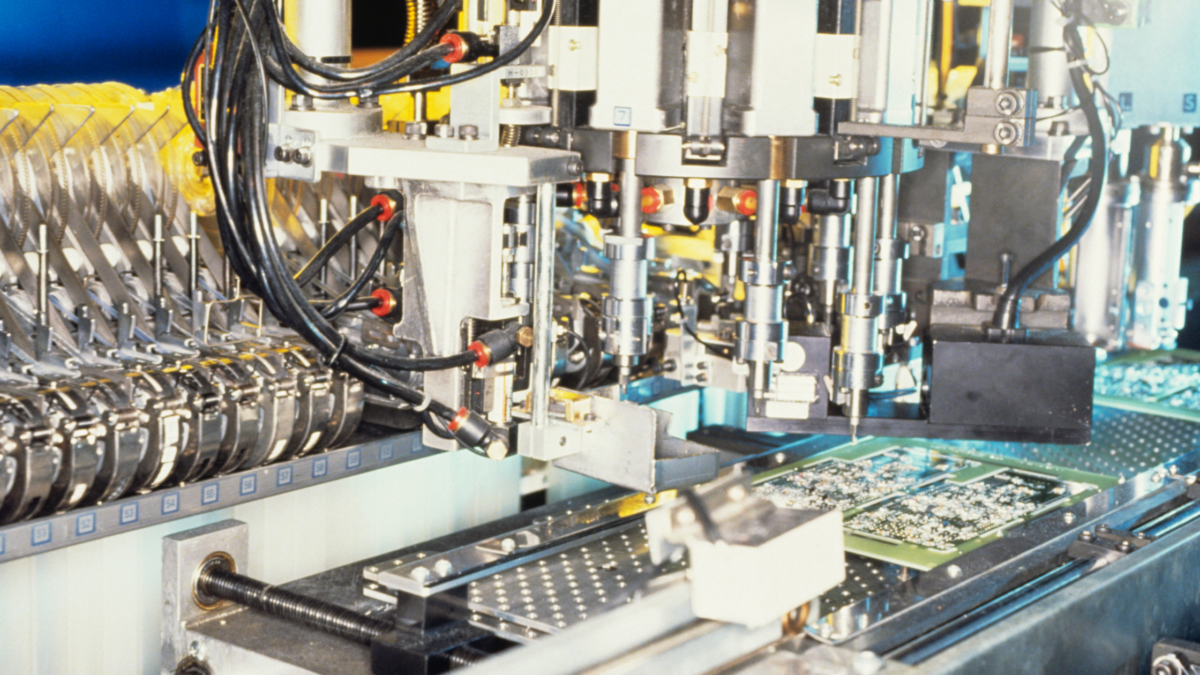
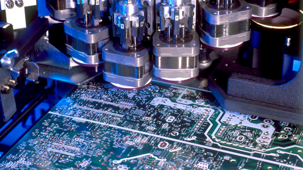
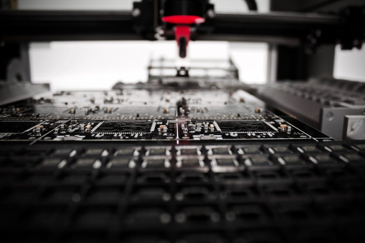
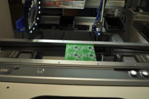
Once solder paste has been applied, the PCB moves to automated pick-and-place equipment.
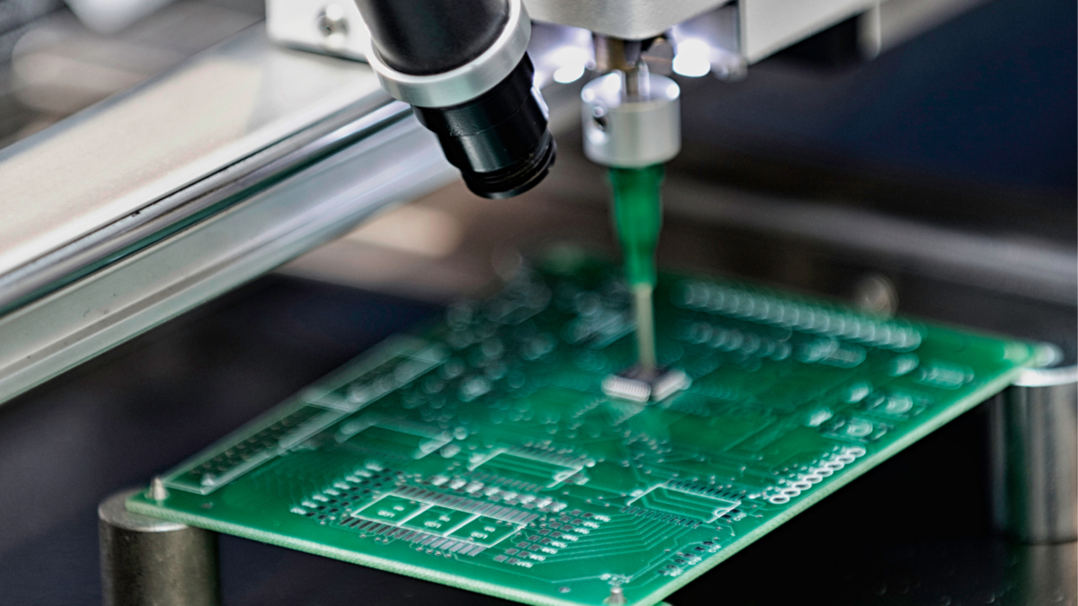
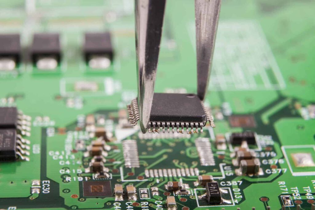
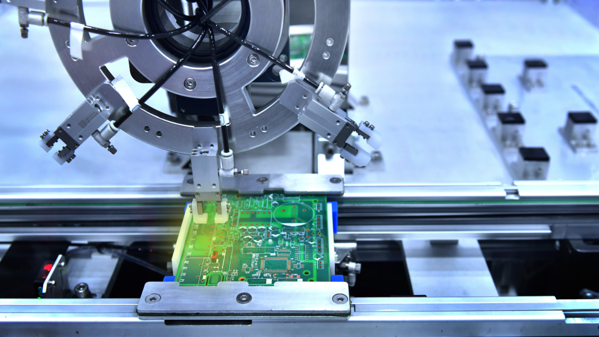
These machines take surface-mount devices from reels, trays, or other packaging and position them on the circuit board according to programmed placement data.
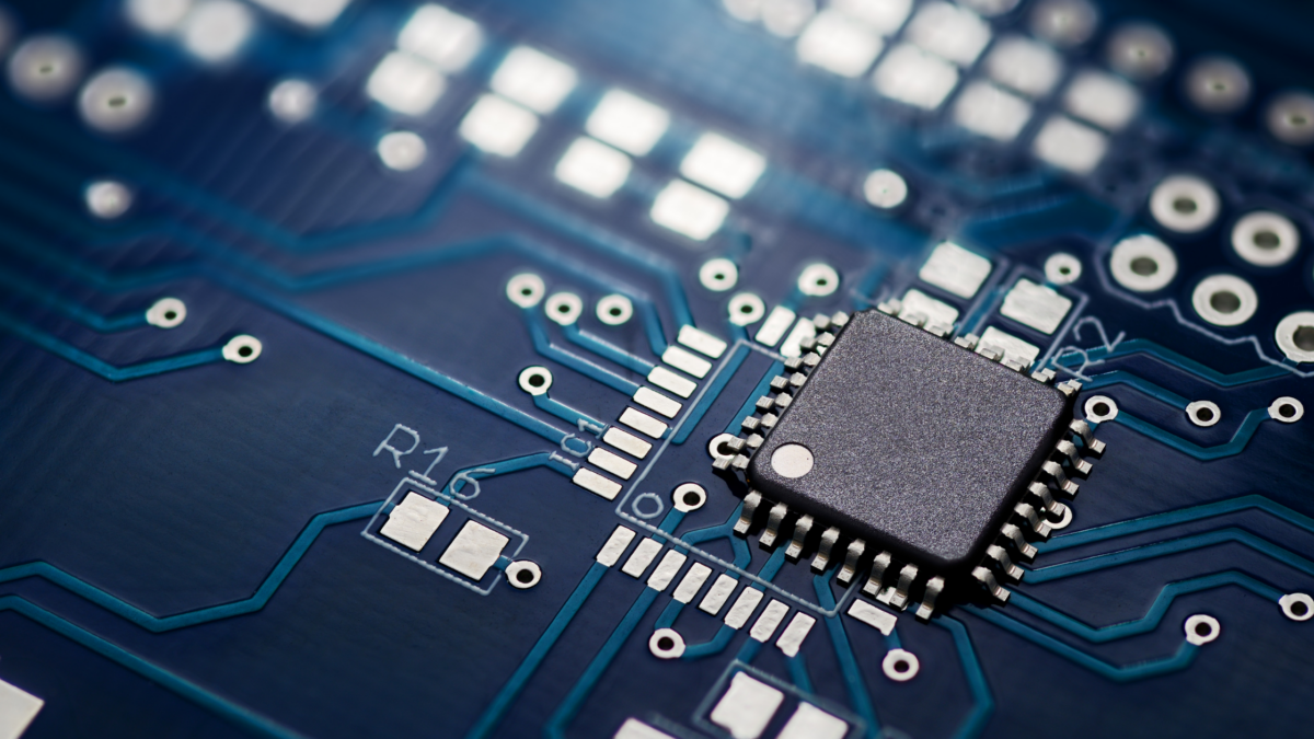
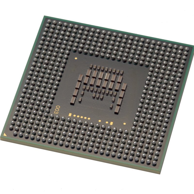
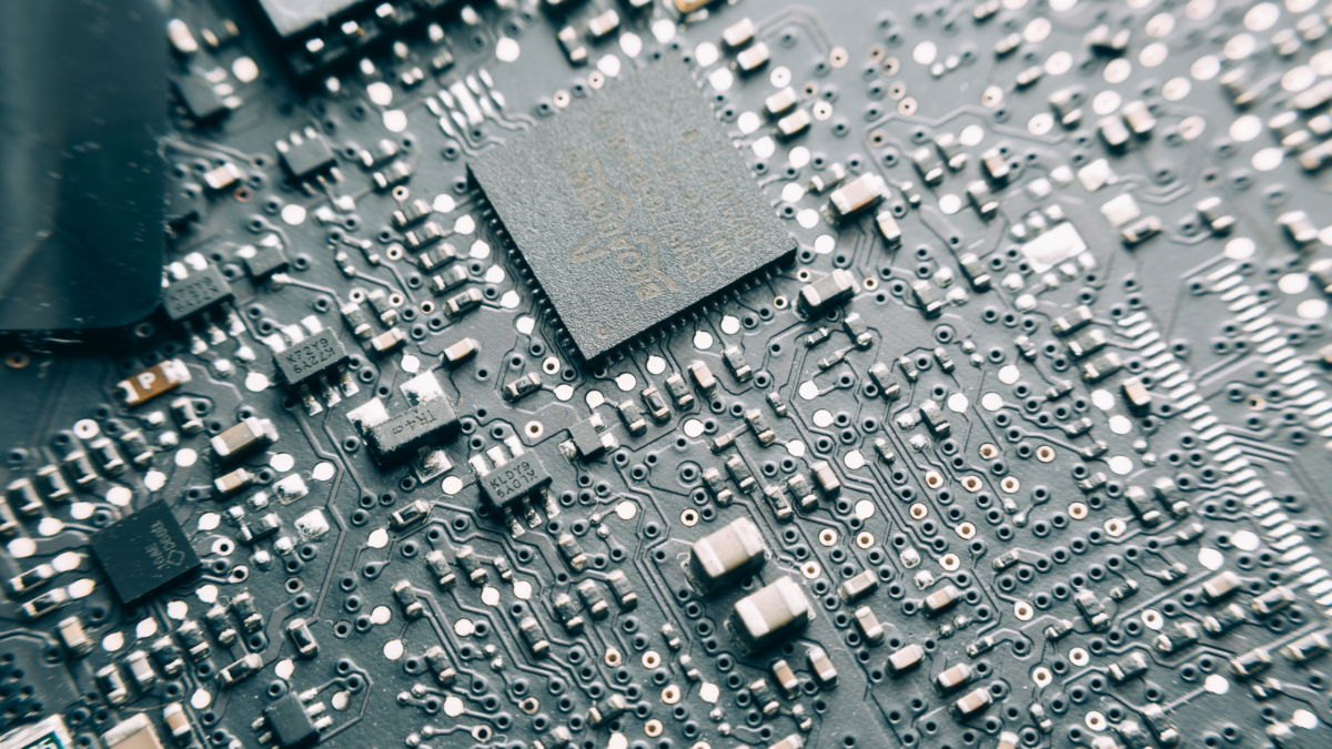
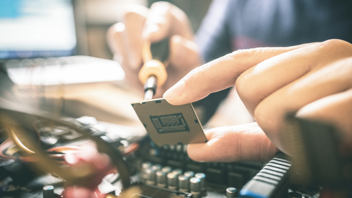
Surface mount technology, commonly called SMT assembly, allows manufacturers to place tiny components efficiently and accurately. Modern assemblies may include resistors, capacitors, integrated circuits, fine-pitch components, BGAs, micro BGAs, and many other package types.
5. Reflow Soldering
After component placement, the PCB passes through a controlled reflow oven.
The board travels through carefully managed temperature zones that gradually heat the assembly. The solder paste melts, or “reflows,” around the component leads and pads. As the board cools, the solder solidifies and forms permanent electrical and mechanical connections.
A controlled reflow profile is important because different components and PCB designs respond differently to temperature.
6. Automated Optical Inspection
Component placement is only part of a successful circuit board assembly. The board must also be inspected.
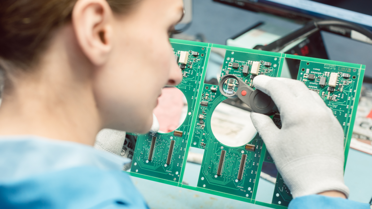
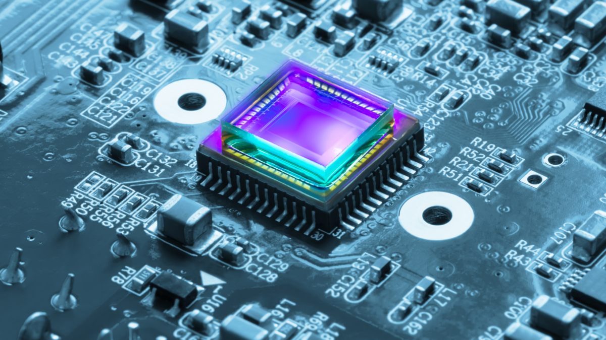
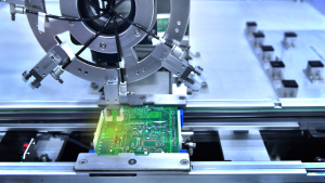
Automated Optical Inspection, or AOI, uses cameras and inspection software to evaluate assembled PCBs for potential problems such as incorrect components, placement errors, polarity issues, or solder defects. A controlled reflow profile is important because different components and PCB designs respond differently to temperature.
At Nova Engineering, automated SMT inspection includes 3D AOI technology, followed by final visual inspection as part of the quality-control process.
7. Through-Hole and Mixed-Technology Assembly
Not every circuit board uses surface-mount components exclusively.
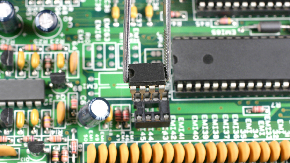
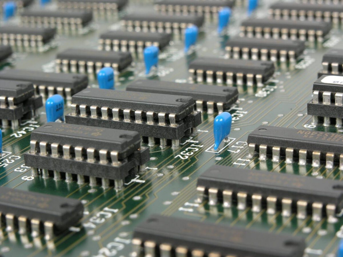
In through-hole assembly, component leads pass through holes in the PCB before being soldered into position. Through-hole technology remains useful for connectors, larger components, and applications where the design requires additional mechanical strength.
Many modern PCBs use mixed-technology assembly, combining SMT and through-hole components on the same board.
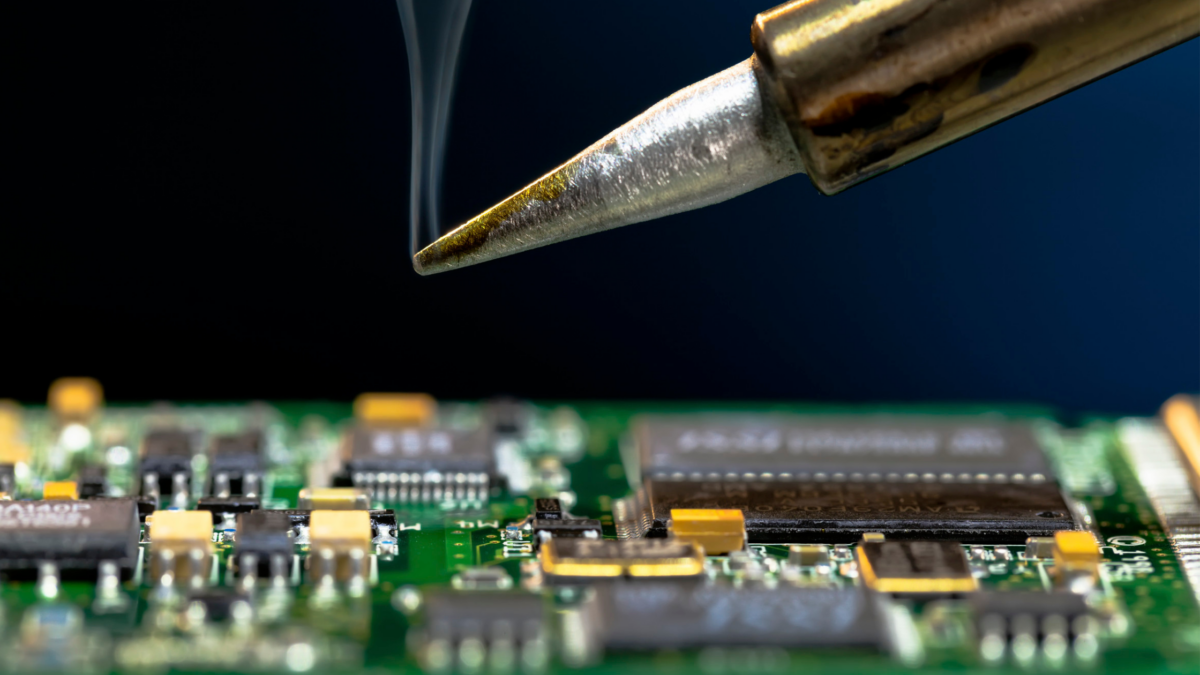
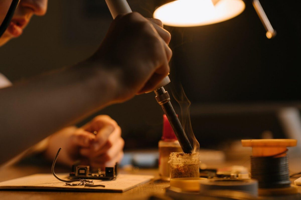
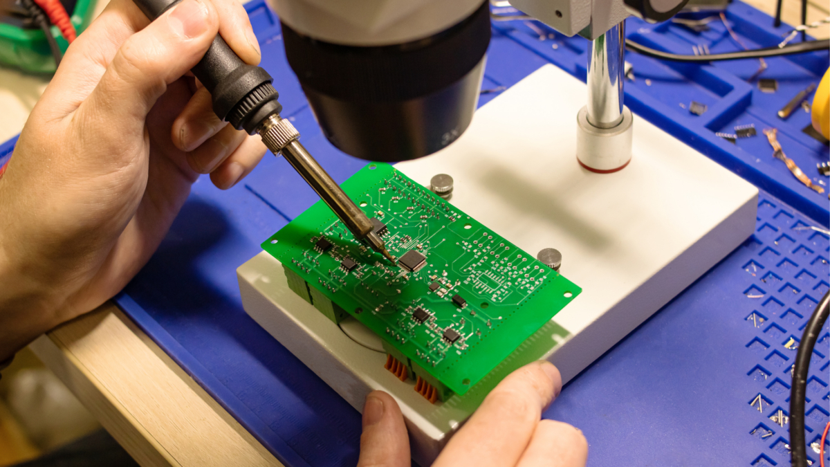
Depending on the design, through-hole components may be soldered manually, through wave soldering, or using other controlled soldering processes.
8. X-Ray and Additional Inspection
Some solder joints cannot be seen with standard optical inspection.
Components such as BGAs, QFNs, and LGAs have electrical connections underneath the component body. X-ray inspection allows technicians to examine these hidden connections for conditions such as shorts, opens, alignment problems, or other soldering concerns that may not be visible from the surface.
Using the appropriate inspection method is especially important as circuit board designs become smaller and component density increases.
9. Testing and Final Verification
The circuit board assembly process does not end when everything has been soldered.
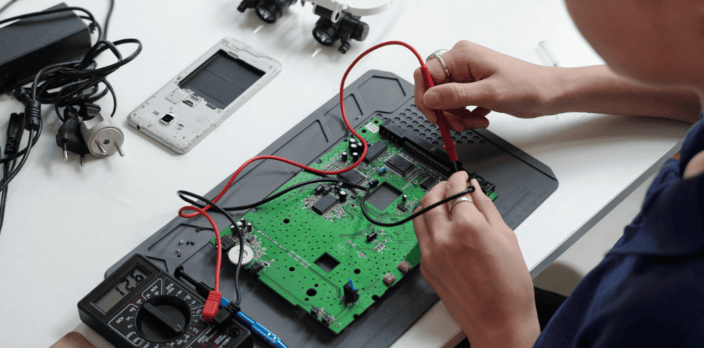
Finished PCB assemblies may undergo visual inspection, electrical checks, or customer-defined functional testing depending on the project requirements. Testing helps verify that the completed assembly operates according to its intended design before it moves into a larger system or final product.
Documentation and traceability can also be important, particularly for industries with demanding quality requirements.
Why Quality Matters
A PCB can be designed correctly and still fail if it is assembled poorly.
Incorrect component orientation, solder defects, contamination, damaged components, inadequate thermal control, or hidden connection problems can affect the performance and reliability of the finished product.
That is why professional PCB assembly combines controlled manufacturing processes with inspection throughout production instead of relying only on a final check.
How We Can Help
At Nova Engineering, we have been providing circuit board assembly and PCB assembly services for more than 35 years from our Denver, Colorado facility.
Our capabilities include prototype, turnkey, consigned, and partially consigned PCB assembly for surface-mount, through-hole, and mixed-technology designs. We also use DFM review, automated optical inspection, X-ray inspection, and detailed quality-control processes to help customers move from initial prototypes into production.
Whether you are developing your first prototype or preparing an established design for another production run, choosing the right circuit board assembly partner can help reduce manufacturing issues and keep your project moving.
Contact Nova Engineering to discuss your PCB assembly requirements or request a quote for your next project.
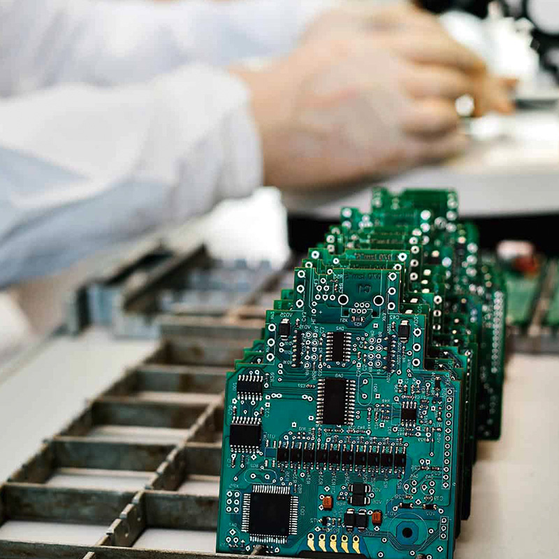

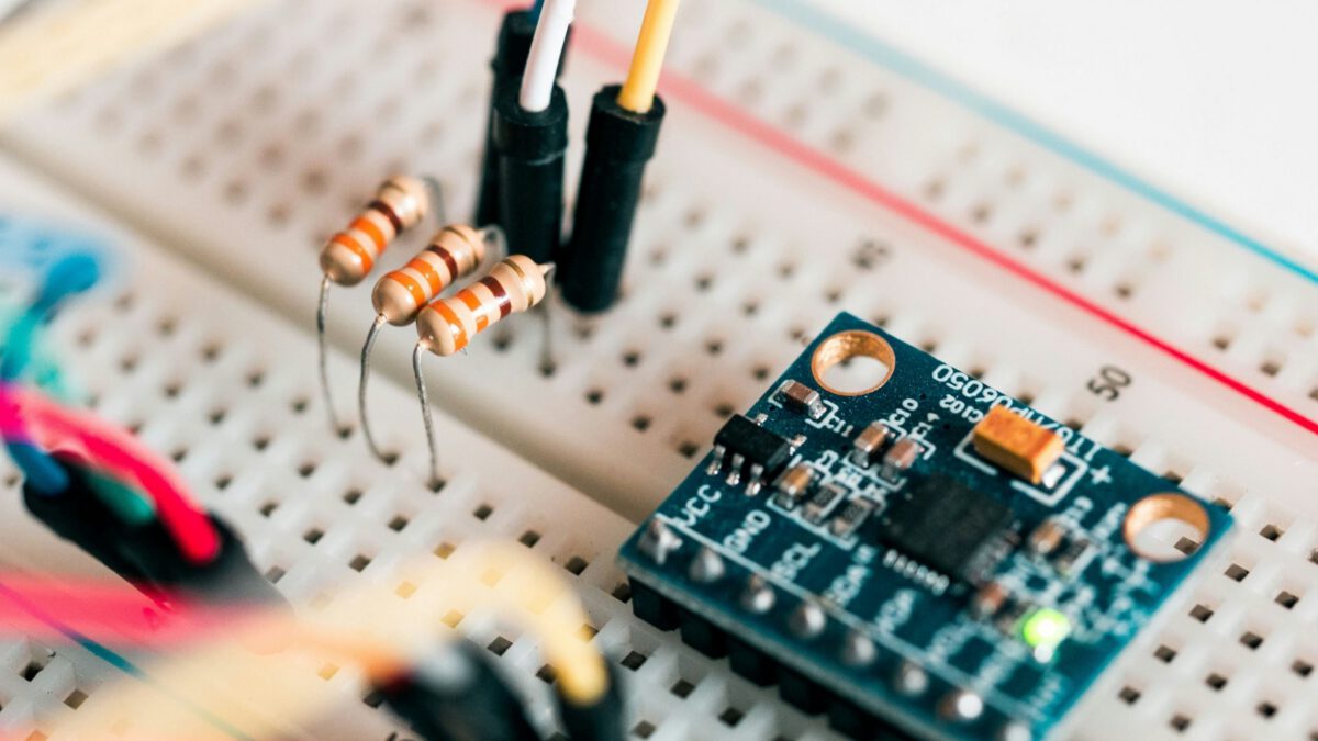
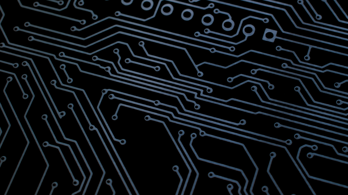
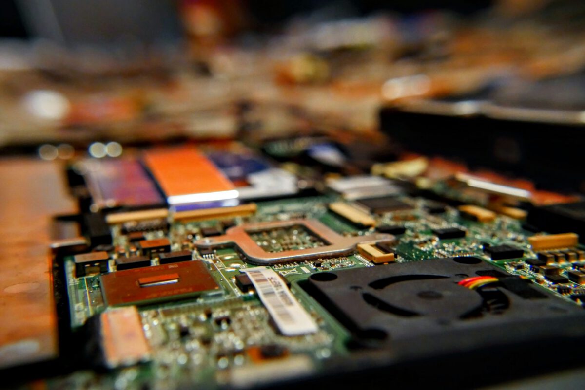
 Simulation and Testing Capabilities: Reliable simulation and testing features are essential for verifying that your PCB design will function as intended before moving to production. OrCAD is known for its powerful simulation tools, which are crucial for identifying potential issues early in the design process. To learn more about how we ensure quality in every project, check out our Quality Assurance page.
 The 1950s brought a major shift in the history of circuit boards with the advent of transistors. Unlike vacuum tubes, transistors were small, reliable, and efficient. This innovation allowed PCBs to shrink in size while increasing in complexity and reliability. Electronics could now be manufactured for home use, enabling the rise of consumer electronics.