
The circuit board assembly process is the heart of nearly every electronic device we use today—from smartphones to medical equipment. If you’ve ever wondered how these complex gadgets come to life, it all starts with a precise and highly technical process that transforms raw components into fully functional circuit boards.
In this guide, we’ll break down what the circuit board assembly process is, how it works, and why proper assembly is essential for a device’s performance and reliability.
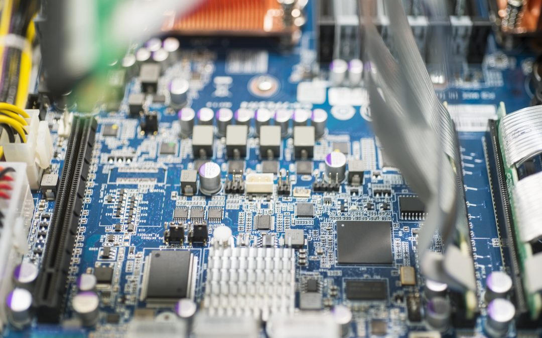
What Is a Circuit Board?
At the core of the circuit board assembly process is the printed circuit board, or PCB. A PCB is a flat, typically green or blue board that holds and connects all the electronic components necessary for a device to function. While it may look like a simple piece of plastic, it’s actually a carefully engineered multi-layered structure composed of copper layers, insulating materials, and a protective coating.
These layers form the foundation of the circuit board assembly process, serving as both the physical platform and the electrical pathway for components like resistors, capacitors, and microchips.
The Layers Behind the Circuit Board Assembly Process
A standard circuit board used in the circuit board assembly process may have anywhere from 2 to 50+ layers, depending on the complexity of the device. These layers include:
-
Top and Bottom Layers: These are the surfaces where most components are mounted during the circuit board assembly process. They also contain antennae in certain applications.
-
Power and Ground Planes: These layers distribute power and grounding across the board.
-
Signal Layers: Internal layers route communication signals between components.
-
Insulation Layers: Fiberglass and epoxy resin insulate the copper layers and prevent electrical shorts.
-
Solder Mask and Silkscreen: The outermost coatings used to protect the copper and guide component placement.
Each part of this multi-layered system plays a critical role in the circuit board assembly process, ensuring electrical functionality and durability.
Step-by-Step: The Circuit Board Assembly Process
Now let’s walk through the key steps involved in the circuit board assembly process:
1. Solder Paste Application
The process begins with applying solder paste to the board using a stencil. This paste helps secure components to the board once heat is applied.
2. Automated Component Placement
High-speed machines then place components like ICs, resistors, and capacitors on the board with extreme precision—an essential phase of the assembly process.
3. Reflow Soldering
After placement, the board goes through a reflow oven, which melts the solder paste and creates permanent electrical connections.
4. Inspection and Quality Control
The circuit board assembly process includes both visual and automated optical inspections to detect misalignments or soldering defects.
5. Through-Hole Component Insertion (if needed)
Some designs use through-hole components, which are manually or mechanically inserted and soldered into place.
6. Final Testing
Before a board can move on to the product line, it undergoes functional and electrical testing. This stage of the assembly process ensures that every connection works as expected and that the board meets performance standards.
Why the Circuit Board Assembly Process Matters
A reliable assembly process is essential for ensuring the final product works correctly and consistently. Poor assembly can lead to:
-
Device malfunctions
-
Shortened product lifespans
-
Safety risks
-
Costly recalls and repairs
That’s why quality control, precision, and proper testing are key throughout the circuit board assembly process.
The Backbone of Modern Electronics
The circuit board assembly process is what transforms raw materials and components into the electronic brains of modern devices. Whether you’re using a smartphone, a smart thermostat, or industrial automation equipment, it’s all powered by a carefully assembled circuit board.
Understanding the assembly process helps you appreciate the complexity behind the technology we rely on every day and highlights why choosing a trusted manufacturing partner like Nova Engineering is critical to success.
Originally Published: 9/13/2021
Recent Comments