Circuit Board Assembly – How Is It Manufactured?

The assembling and manufacturing processes begins with the solder paste that sticks to the board used for connecting electrical components. Following that, the process moves to the “pick and place” procedure of the components. In simple words, the entire circuit board manufacturing process includes soldering, inspection, and testing. After the manufacturing process is complete, experts need to send feedback depending on any failures or difficulties with the help of intelligent technology. All stages of the manufacturing process are under monitoring.

With that said, most manufacturers ensure high quality through supervised operations. In the post below, we will discuss the assembly and manufacturing process based on surface-mounted technology for PCBs.

Two Important Stages of the Assembly Process

Check out the two most important stages of the assembly process that lead to high-quality manufacturing:

·         Solder Paste

The first step involves using solder paste on the board using a process that’s similar to screen-printing. The only difference is that it relies on a stainless-steel stencil, which is positioned over the PCB. This way, the assemblers only apply the solder paste to particular parts of the circuit. These areas with the solder paste are where the components will sit.

·         Pick and Place

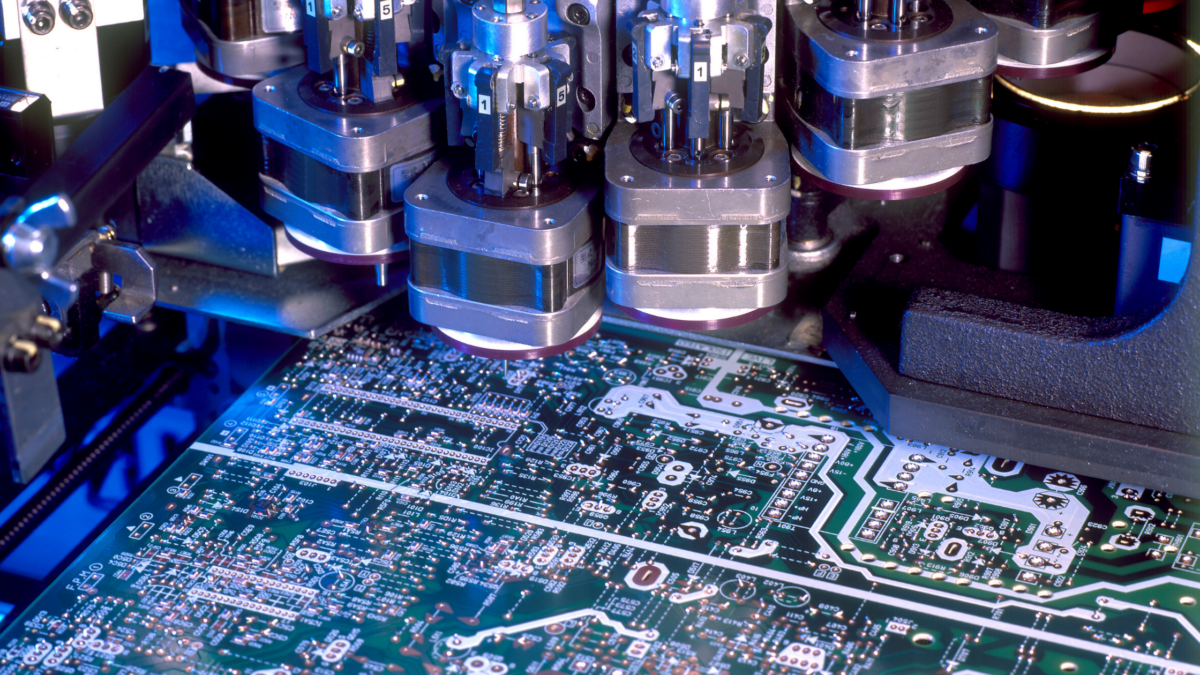
All boards coming from the assembly process containing solder paste will move to the pick and place process. There, a machine containing component reels will dispense and place components on the board safely where required.

Let’s take a simple overview of the entire manufacturing process below!

Simple Overview of the Manufacturing Process

Here, we will discuss the entire manufacturing process in the most simplified manner for greater comprehensibility. Since the boards aren’t jolted, the solder paste must be effectively and efficiently pasted on them. Why’s that? Well, the quality placement of solder paste will also keep the electrical components in a fixed position on the board.

For wave-soldered boards, pick and place machines add tiny dots of glue to hold the components in place. But, this makes all the repair processes cumbersome because the glue can get messy and interfere with the boards’ components.

The printed circuit board design information allows the pick and place machines to learn about the position and all component information. This allows the machines to program the components as per the requirements. Here are the different stages of the manufacturing process that you must know about:

·         Soldering

The boards pass through the soldering machine once the assembly process of placing components on the boards is complete. However, you must know that some processes involve the use of wave soldering machines, i.e., not for the latest PCBs that are powered by surface-mount components. Since the wave soldering machine provides the solder paste, it doesn’t need to be added separately to the board. As the latest PCB fabrication and release involves surface-mounted technology, the use of reflow soldering techniques is more widespread.

·         Inspection

Once the boards pass through a soldering process, they require careful inspection. This is most important to the overall manufacturing process. Firstly, it ensures high-quality manufacture with defects identified on the spot. Secondly, as failure is detected, the rest of the production can be held and made correct by rectifying the respective errors. Since the surface-mounted PCBs use hundreds or even more components on the insulating board material, a manual inspection can be tiring and time-consuming.

For that reason, automatic optical inspection is a more viable option. From misplaced and wrong components to poor joint placements, the respective optical inspection system can detect a range of failures and errors.

·         Testing and Feedback Report

Before leaving the factor, the manufacturing experts perform a test to make sure that all PCBs are functional and high-quality. Furthermore, sending the feedback report allows the manufacturing to suffer from fewer failures and errors.

Conclusion

The detailed post above contains the entire manufacturing process in a simplified way. All essential processes of assembly and manufacturing have been discussed. For your information, the entire production process is considerably optimized so that the level of defects is low. That’s one of the major ways manufacturers ensure high quality. The abovementioned operations of the manufacturing process are quite important to meet the growing demands and expected quality for high-end technology placements.

Circuit Board Assembly – How Is It Manufactured?

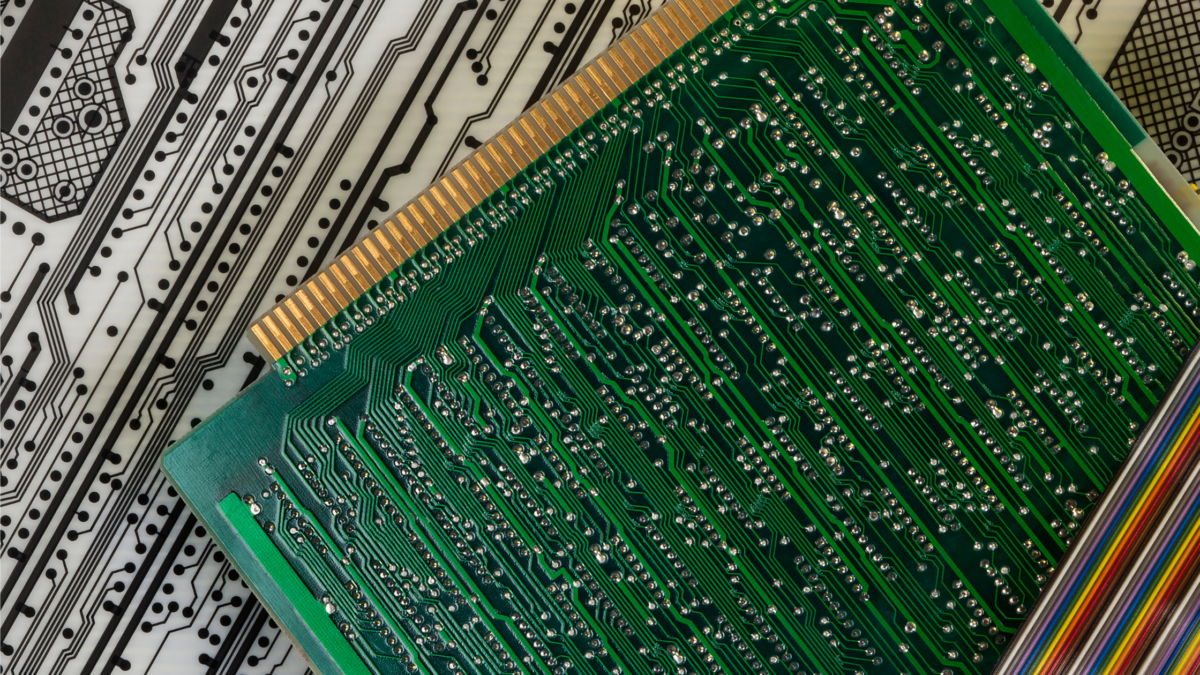
The assembling and manufacturing processes begins with the solder paste that sticks to the board used for connecting electrical components. Following that, the process moves to the “pick and place” procedure of the components. In simple words, the entire circuit board manufacturing process includes soldering, inspection, and testing. After the manufacturing process is complete, experts need to send feedback depending on any failures or difficulties with the help of intelligent technology. All stages of the manufacturing process are under monitoring.

With that said, most manufacturers ensure high quality through supervised operations. In the post below, we will discuss the assembly and manufacturing process based on surface-mounted technology for PCBs.

Two Important Stages of the Assembly Process

Check out the two most important stages of the assembly process that lead to high-quality manufacturing:

·         Solder Paste

The first step involves using solder paste on the board using a process that’s similar to screen-printing. The only difference is that it relies on a stainless-steel stencil, which is positioned over the PCB. This way, the assemblers only apply the solder paste to particular parts of the circuit. These areas with the solder paste are where the components will sit.

·         Pick and Place

All boards coming from the assembly process containing solder paste will move to the pick and place process. There, a machine containing component reels will dispense and place components on the board safely where required.

Let’s take a simple overview of the entire manufacturing process below!

Simple Overview of the Manufacturing Process

Here, we will discuss the entire manufacturing process in the most simplified manner for greater comprehensibility. Since the boards aren’t jolted, the solder paste must be effectively and efficiently pasted on them. Why’s that? Well, the quality placement of solder paste will also keep the electrical components in a fixed position on the board.

For wave-soldered boards, pick and place machines add tiny dots of glue to hold the components in place. But, this makes all the repair processes cumbersome because the glue can get messy and interfere with the boards’ components.

The printed circuit board design information allows the pick and place machines to learn about the position and all component information. This allows the machines to program the components as per the requirements. Here are the different stages of the manufacturing process that you must know about:

·         Soldering

The boards pass through the soldering machine once the assembly process of placing components on the boards is complete. However, you must know that some processes involve the use of wave soldering machines, i.e., not for the latest PCBs that are powered by surface-mount components. Since the wave soldering machine provides the solder paste, it doesn’t need to be added separately to the board. As the latest PCB fabrication and release involves surface-mounted technology, the use of reflow soldering techniques is more widespread.

·         Inspection

Once the boards pass through a soldering process, they require careful inspection. This is most important to the overall manufacturing process. Firstly, it ensures high-quality manufacture with defects identified on the spot. Secondly, as failure is detected, the rest of the production can be held and made correct by rectifying the respective errors. Since the surface-mounted PCBs use hundreds or even more components on the insulating board material, a manual inspection can be tiring and time-consuming.

For that reason, automatic optical inspection is a more viable option. From misplaced and wrong components to poor joint placements, the respective optical inspection system can detect a range of failures and errors.

·         Testing and Feedback Report

Before leaving the factor, the manufacturing experts perform a test to make sure that all PCBs are functional and high-quality. Furthermore, sending the feedback report allows the manufacturing to suffer from fewer failures and errors.

Conclusion

The detailed post above contains the entire manufacturing process in a simplified way. All essential processes of assembly and manufacturing have been discussed. For your information, the entire production process is considerably optimized so that the level of defects is low. That’s one of the major ways manufacturers ensure high quality. The abovementioned operations of the manufacturing process are quite important to meet the growing demands and expected quality for high-end technology placements.
A Brief History on PCBs

The printed circuit board enables all electrical components to work together in order to function all electronic devices that you see today. The printed circuit board, therefore, optimizes the functionality of electronics and has taken over many roles throughout history.

For instance, it primarily acted as a component holder. Then, it became an alternative to unnecessary wiring and cabling. Today, it is the superstructure for high-speed design.

The Birth of the First PCB

In 1940, the first printed circuit board was produced, and it was for the proximity fuse for the artillery shells. This was the middle of World War 2, and Great Britain was at war with the Nazis. Since they were on the back foot, the intelligence committee of Britain came up with a proximity fuse. This was inserted into the shells and exploded as it came near an object.

This invention was revolutionary for its time as it included a circuit that could detect when it was close enough to something and then explode. The UK was very successful with this invention. Moving forward to the post war era, the war ended in 1945. And in 1947, the first transistor was invented.

This transistor revolutionized the way people viewed electronics and changed the world of electronics, pushing forward great success. During this period of time, the first application of the transistor was the television set, and it was popular.

The circuit board inside the television set looks nothing like the printed circuit boards of today. Instead, it looked like individual components were strapped in, and wires were soldered to each of the component’s leads.

This was a very manually intensive way of building an electronic device, and it may have taken a couple of days for manufacturers to make them. If someone is sitting there and soldering all day long, you begin to wonder about the quality of the product as well.

Introduction to Etching Copper

In 1956, the US army patented an etching copper board. At that time, this was a very unusual way of making a circuit. The idea for etched copper involved getting a plain copper surface and then etching out the traces you’d want. After that, attach leaded components, or “through-hole components,” and you would put them through the board.

This was revolutionary because it turned a difficult and time-consuming process into one that you could complete in 20 minutes. This was a giant leap forward in electronics manufacturing. Granted, you only had one-sided boards at that time, but it served the purpose of getting from point A to point B.

PCB Today

A printed circuit board today is highly optimized because of miniaturization. Today, when you look at a highly specialized circuit board, you find really tiny components that neatly align to a board that connects all of the ports, headers, and sockets. These traces on printed circuit boards have made all of the modern electronics possible.

Before they became widespread, connecting components inside an appliance was a time-consuming and unorganized process. The idea of embedding wires on flat fiberglass made it possible to minimize highly complex electronic devices, such as smartphones and laptops.

Moreover, the printed circuits boards of today also have layers of copper on both sides of the fiberglass board, making them hold more components.

To Conclude

As you can see, the technologies of printed circuit boards have come a long way, and today they serve the most important functions for humanity, driving the wheels of commerce and information.


Differences between Surface Mount Assembly and Electro-Mechanical Assembly

There are different ways you can assemble micro-electrical components on a printed surface board. And the surface mount assembly is more popular than the electro-mechanical assembly.

Nonetheless, each has its own advantages and disadvantages. To understand the difference between the two, you must have an overview of both methods.

Surface Mount Assembly

This method is a way to produce electrical circuits by directly placing or mounting the components on the surface of printed circuit boards. In this method, all components or devices are mounted on the board with the help of a solder mask.

If the assembly method is surface mount assembly, the production process will be incredibly fast. However, it has many drawbacks as well.

For instance, even though the production process significantly speeds up, it simultaneously increases the risk of defects during the assembly process.

This is largely because of the miniaturization of the components, along with the denser packing of boards.  In these conditions, testing and inspection for failures and errors become increasingly critical in the manufacturing process. The manufacturing of printed surface boards using surface mount assembly includes a sequence of processes.

The assembly process starts with the application of solder paste. This is the substance on which the electrical components are mounted. After you apply the solder mask to the board, you move forward to placing the components. This can be done manually or with the help of machines.

This process then moves ahead to the reflow soldering process, after which all the excess solder is cleaned. After these steps, the surface mount assembly process is complete, and you can move on to the testing phase of the printed circuit board.

Electro-Mechanical Assembly

Electro-mechanical assembly is heavily reliant on machinery and other automatic drive units. Electronic products consist of interconnections and many components. These components can also be devices that alter the flow of electricity, such as resistors, conductors, and capacitors.

The circuit board assembly is, therefore, the driving force of most electronic products since it provides the channel through which electricity can pass to all components. There are two ways components can mount to the circuit boards. And most electro-mechanical assembly processes focus on the through-hole process.

In this process, each component comes with leads, which fit inside the through-holes of the circuit board.  These types of components are very old since the through-hole method has been used for a very long time.

Which One is Better?

In terms of cost, surface mount assembly is more cost-effective for a number of reasons. One of the reasons is that SMT components are much easier to find. Another reason is that there are many services that manufacture a surface-mounted printed board exactly to your specifications.

Not to mention, for the low price that it offers, it also provides better design quality and speed. Moreover, testing through-holes can be difficult and may require specialized testing equipment, which will, in turn, have you spend more on testing.

Final Words

Electronic assembly process techniques are sometimes integrated into the surface mount assembly process, depending on the product you deal with. Therefore, it is difficult to say whether one is better than the other because projects can vary vastly.

However, it is fair to say that the through-hole method is outdated and has more drawbacks than the surface mount technology.

Important Considerations for PCB Assembly

Designing and assembling PCBs is an incredibly valuable skill. Nowadays, it is a process that is easy to learn and implement, as long as you are willing to invest your time in it. Back in the early days, the PCB assembly process was time-consuming. However, today, you have many software programs that allow you to design them and get them delivered to your doorstep.

Nonetheless, any mistake that you make in your design can be very costly to you. This is because your design will dictate the assembly process, along with the functioning of the board. With a nonworkable board, the electronic device will also suffer from malfunctions and errors.

To avoid these errors, you must take certain things into consideration when assembling and designing a PCB board.

Do not be Impatient

A printed circuit board is a piece of technology that has a precise and sophisticated design. Each detail is thought-through and requires careful considerations. This is why you must never be impatient in any of the PCB assembly processes.

Most people make the mistake of being impatient when they are placing components on the board. According to professional PCB designers, it is integral to have most of the time go to components placement when designing and assembling the PCB.

This is true because the placement framework will ultimately determine the outcome of the PCB design. The trick is to avoid overlapping the rubber panels. Moreover, you have to keep adjusting each placement until there is no overlapping.

When designing, if you spend enough time on your digital component placement, your routing will be significantly easier.

Consider Routing Directions

Once you complete the component placement, then you will have to move forward to routing. For this, you will have to decide the routing direction of a particular layer before laying down the traces.

Make sure that you set the right directions as even the slightest inconsistencies in direction can lead to complete design failure.

Narrow High Current Traces

Make sure that you do not develop the habit of using the same width for all the traces in your design; well, you do not want to do that. Make sure that your traces can withstand the maximum voltage.

If a particular trace carries a higher trace width than the other traces in your design, make sure to increase the width for the others as well.  High-width traces ensure proper heat dissipation.

Make use of Copper Pour

Making PCBs involves etching the unused copper and leaving the traces intact. Copper pouring means that you have to use unused copper for any signal instead of etching it out. You have to do it by creating spaces for traces and pads.

Commonly, people will use them for power signals or ground signals. This offers a low impendence path for the current and also makes connection much easier.

Pay Attention to Spacing

Most designers do not consider the importance of spacing and end up making a flawed printed circuit board. Proper spacing requires much more effort and consideration.

Thus, designers should be well aware of the adequate spacing requirements for a particular circuit.  You should also consider the assembly of components to ensure proper spacing.

Final Thoughts

These are just a few of the many considerations that you should take when performing a printed circuit board assembly. As you can see, the design process is very important as it can account for an efficient and safe assembly.

Practices that Account for Flawless PCB Assembly

Printed circuit boards are the basic parts of all electronic components, as they are responsible for the smooth flow of electricity inside the device. Without this distribution of electricity, all electronic components will fail to function.

Nonetheless, for a printed circuit board to perform its job efficiently, it is important that it works efficiently without any flaws. For the printed circuit board to work well, its assembly process must adhere to some important set of practices and standards which help make the PCB functional and smooth.

Inspect the Materials

Your PCB is as good as the quality of materials and components that you use. Professional PCB assembly units place a high priority on the material they use when putting together a PCB, as this can be critical.  You want to make sure that you place a high value on quality control when assembling the components on the board.

Maintaining quality requires inspection, testing, and verification of several components and processes involved in the PCB assembly. For instance, you have to take into account factors such as the quality, model number, and data code and make sure that it matches with the BOM.

Inspecting the material and components will involve running multiple tests. These tests can include sample testing, material operational testing, and others.

Furthermore, you can also check whether the components are oxidized, deformed or damaged before applying them to the assembly.

DFM Check

This is another way you can make sure that your PCB works smoothly and efficiently. Running a design that focuses on DFM checks allows manufacturers or people working on PCB projects to create a seamless assembly and identify errors that can be potentially problematic at later stages of assembly.

Furthermore, this test can unveil many flaws pertaining to component polarity, spacing, footprint corroboration, and more.

By doing so, a DFM test can significantly decrease the cost of manufacturing and speed up the delivery process as well.

Not to mention, by revealing the flaws to you in time, the DFM test also saves the time you need for the rework process. Ultimately, all of these benefits translate into improving the quality of the product significantly.

Inspect Solder Paste

Solder paste application is crucial to the PCB assembly process. The solder paste is the material that holds the components on the board with strength. Application is done with the help of a machine, as it holds the stencil over the board, after which the solder is poured on the surface of the board.

These open spaces are where the surface mount components are placed. Thus, people working on circuit board assemblies should ensure that the solder mask they use has good composition so that it is applicable for assembly.

An inspection of the printed circuit board should always follow the solder mask test and application. This determines whether the board will hold all the components.

Sound Communication

When designing and creating a PCB for another person, it is important to understand what the other person is exactly looking for. Setting a clear line of communication will lead to a PCP that fulfills all the necessary needs and preferences.

Finally

With the use of advanced technologies, you can create a PCB that ticks all the boxes relating to reliability and accuracy. These technologies take shape in the form of tests and inspection tools. When you run your PCB through some of the tests above, it guarantees a final product that is flawless and seamless.

The Evolution of Printed Circuit Boards

Since the manufacturing of the first printed circuit board, many developments and advancements have taken place. Some of the most significant developments in the manufacture and design of PCBs have made it possible to utilize modern technology today.

PCBs are essential since they are the main component of electrical equipment. They provide a physical base through which the connections between electronic components establish. All electronic devices around us have PCBs, including TVs, computers, radios, mobile phones, etc. But do you know what led to the success of modern technology? Looking at the evolution of important PCBs will help you get the idea.

Beginning of Printed Circuit Boards

The first iterations of the printed circuit boards took place around the 1920s. At this time, the PCBs could use anything as their base material. If that’s not surprising at all, some people tried to use wood as well. Experts drilled the material to create holes which they later used to place bulky wires on the board. During the initial production, the use of bolts and buts replicated the use of rivets. Contrary to popular belief, the initial circuit boards were nothing similar to what we see and use today. While PCBs weren’t as successful then, they were useful for their functions in radios and gramophones.

PCBs’ Initial Development

It wasn’t until the 1960s that the use of material for producing the physical base of the circuit shifted from wood to other types of material, including the resin. Moreover, the circuits before comprised a one-sided outlook; this entails that the board components were on one side while the entire circuitry remained on the other. Though, it was still a major improvement in contrast to the heavy wiring that took place before. Further down the road of development, the US introduced an assembling procedure for electrical circuits that turned out to be a great help in how experts were handling PCBs. The process had a few essential aspects. One of them was drawing a wiring pattern over a zinc plate to print the electrical circuit on it accurately.

Later in the years, the developments helped to make the PCBs corrosion-free. It was around this time that the production of multilayer PCBs took place. Following that, the PCBs went through miniaturization. This didn’t mean that there were compromises in the complexity or functional efficiency of the PCBs. In fact, they became more efficient and responsive to the changes.

Miniaturization with Complexity

PCB experts are always looking to increase the functional capacity and efficiency of the PCB while ensuring that they are much smaller in size. The use of different technologies is more common today. CAD became the go-to option for designing PCBs. With the use of CAD, experts designed circuit boards that were greater in functionality and efficiency. Furthermore, with the efficiency, the complexity of design and programming also increased. Meanwhile, the size of the PCBs remained small and compact. Apart from that, the circuit board industry continues to develop new models and technologies for use in various applications around us.

Conclusion

While you may not know everything regarding PCBs, you can surely understand their use and scope by looking at the technological advancements. PCBs are nearly a 100-year-old development that is still helping us build more efficient and effective technology. In short, without a PCB, you wouldn’t be reading this information on your digital device.

Reference Links:

https://www.eurocircuits.com/blog/the-history-of-printed-circuit-boards/

https://www.theengineeringprojects.com/2019/06/evolution-of-pcb-printed-circuit-board.html

https://www.clarydon.com/the-evolution-of-printed-circuit-boards

https://www.tempoautomation.com/blog/a-brief-history-of-printed-circuit-boards-design-and-manufacturing/

https://www.autodesk.com/products/eagle/blog/history-of-pcbs/

Everything You Need to Know About Circuit Board Assembly!

Most of the electrical appliances that run our lives on a daily basis include about 300 feet of tiny wires inside. This wire is the main component that adds connectivity inside an electrical product. It allows all the other small components in an electrical appliance to work seamlessly together.

The more complex an electrical appliance is, the larger the number of components and the wire inside it. However, you may be wondering where this wire is located. Well, this is where the printed circuit board assembly comes into play.

What is a PCB?

The printed circuit board or PCB is the small circuit board inside most electrical appliances. They are either green or blue and at first glance, they look like ordinary pieces of scrap plastic. But in reality, they are actually a multi-layered board that consists of an abundance of copper wires.

This scrap of flat metal is the surface on which manufacturers will precisely and carefully place all the essential components using expensive heavy machinery. Along with that, small copper wires will connect between the components and provide the necessary connectivity that occurs between all the components. This connectivity allows the components to work together and as a result, this paves the way for an electrical appliance to function.

What is inside?

The printed circuit board consists of ten conductive layers. The top and bottom layers of the Circuit board assembly make for surfaces on which manufacturers will mount components and they also act as multiple antennae. Moreover, each of these components on the circuit board requires plenty of power and ground and the PCB has entire layers that are only responsible for providing power and ground.

They are also aptly named power planes and ground planes due to their specialized role. Other ground planes that make the circuit board assembly serve the purpose of electromagnetic shielding and heat dissipation. The remaining four middle layers carry all the communication traces, which means that they carry all the signal wires.

Each of the conductive layers is copper, and between these conductive layers, there is insulating fiberglass, along with an epoxy resin that protects against the flow of electricity between the layers. A common PCB has a total of ten conductive layers, however, in a more technical and complex application, the layers can range up to 50 or more layers.

On the other hand, you may also find a PCB board that is simpler, with only two layers. Not to mention, on the top and bottom layers of a PCB, you will find a coat of solder mask, which offers a surface on which manufacturers will place components using high-tech machines. On top of the soldering mask is the silkscreen, which is nothing but the ink that indicates the placements for components by marking the circuit board.

The Assembly Process

After all the components of the PCB are manufactured, they need to be assembled before the PCB can go into the production line. This assembly process will involve the application of solder masks, automated component placement, along with the electrical testing of the bare board.

Final Thoughts

Printed circuit boards are more widely used inside computing devices, and since each model of smart phones and laptops along with other devices are different, the shapes and designs of circuit board assembly also differ vastly. Overall, it is fair to say that they are integral components of the modern technical era, and without them, none of the highest technical appliances can function.


How does Automated Trace Routing Work in PCB Design

Every electronic device that you use consists of over a hundred meters of wires, along with dozens of small copper components. These components work seamlessly together to run a specific electronic device, whether it is a Smartphone, television, or remote control. 

All of the wires and components perfectly attach to a thin-layered board, or PCB (Printed circuit board). When engineers mount all the components on this surface, it provides an organized framework for all the small structures to communicate with each other. 

PCB DESIGNING 

PCBs consist of conductive material that sits on insulating material, or the substrate. When you categorize PCBs based on this, you get two classifications, the single-layer PCB, and the double-layer PCB. The single-layer PCB includes a one-sided conductive coating, while the double layer has a coating on both sides. 

One of the many ways to decrease the build-up of heat in a PCB design is to widening the traces on the board. This is one of the routing rules out of many that creators follow when designing PCBs. The wider the distance between the traces, the lesser will be the resistance of the flowing current. To calculate trace widths, you can seek the help of online trace width calculators. 

Similarly, you can find methods that encompass the manual routing process. In an electronic design, automated trace routing is the way to go amidst modern technological advances.

WHAT IS AUTOMATED TRACE ROUTING?

This is a method of design for the printed circuit board, along with the integrated circuits, or (ICs). This step automates the process of placement when integrating a PCB. The dynamics of this method predicates upon identifying the placement for each active component of a PCB. 

The automated trace routing method allows you to enable an automatic routing system that systematically makes all the placements themselves. You can find auto-routing software such as Altium, which provides users an interface that helps access automated trace routing. 

With the help of automated trace routers, encoders can increase their productivity and not waste their time in manual routing solutions. 

SHOULD YOU USE AN AUTOMATED TRACE ROUTER? 

Auto-routing tools can be of immense help, especially if you are a beginner designer. They have incredible use and benefits for simpler designs. However, skilled and experienced designers that incorporate complex routing placements do not use automated routers. 

This is because the automated routing tools will often not have the complex routing strategy or layout in their systems. Therefore, whether you should use an automated trace routing tool depends entirely on the layout of your PCB, the complexity of your strategy, and the settings that you are particularly looking for.

AUTOMATED TRACE ROUTING ALGORITHMS 

Algorithms ultimately define the function of an automated trace router. They are the fundamental construct of the different routing topologies. In other words, they are a set of instructions that automate the routing process, speeding it up, and making this lengthy task easier. 

The three main algorithms for auto-routing involve random search, directed search, and river routing. Each of these algorithms has its advantages and setbacks and suits each encoder for a different set of tasks. 

TO CONCLUDE

If you are new to PCB design, then auto-routing tools can be emphatic to get you started on your PCB projects. In hindsight, the benefits of an automated trace router outweigh some of the drawbacks, especially if you consider the recent advances in their technology.

PCB Finishes: Immersion Silver

It is a well-known fact that printed circuit boards (PCBs) use copper surface finishes as a common practice. If left unattended and unprotected, copper will deteriorate and oxidize, leaving your circuit board unusable. 

A surface finish plays a vital role in creating an interface between a PCB and its components. Here are two of the main functions of a surface finish.

  • It helps protect the copper-based circuitry
  • It provides you surface that can facilitate soldering during the assembling process of soldering components to your PCB

What Is Immersion Silver?

Immersion silver surface finish is a type that you can apply directly over your printed circuit boards’ copper surface. This surface finish is most commonly used and ideal for metallic dome contacts, aluminum wire bonding, and EMI shielding. 

The thickness of this material is between 5 micro-inches and 12 micro-inches, respectively. Additionally, immersion silver has lasting capabilities for at least a year. 

Immersion silver surface finish does not react to copper the way Tin does. However, if you expose it to the air, it will tarnish; therefore, you must store the circuit boards with immersion silver finish in an anti-tarnishing packaging. 

If you do everything right and store it in proper packaging, the PCB will still be solderable for 6 to 12 months. However, once you have removed your printed circuit board from the packaging, you must make sure that it goes through soldering re-flow within the next 24 hours.

In case you wish to achieve a higher shelf life than gold, plating is the most viable solution. 

Benefits of Immersion Silver Surface Finish

PCBs always come with coated surface finishes. Adding a decent finish enables and ensures decent soldering capability, as well as it protects the copper circuitry of your circuit board from the outside air. There are several types of immersion finishes, such immersion tin, immersion gold, etc.; however, immersion silver is gaining popularity due to certain features it offers. 

It is attracting a lot of attention from the PCB manufacturers. Here are some of the key advantages that declare it to be the preferred material for surface finishing in the circuit board industry. 

  • It allows the proper spreading of solder on its surface, allowing better soldering of circuit board components. 
  • Immersion is one of the RoHS compliant PCB surface finishes, and it is also environmentally friendly. 
  • Compared to OSP “Organic Solderability Preservative” surface finish, the surface with immersion silver finish will demonstrate better resistance to several environmental aging factors. 
  • The immersion silver is a material surface finish that comes with the capabilities to survive multiple re-flows. 
  • Immersion silver has better and enhanced electrical properties. 
  • It produces a flat surface and facilitates strengthened solder joints than HASL surface finish. 
  • Immersion silver is immune to a phenomenon known as a black-pad interfacial fracture. 

All of the advantages mentioned above make immersion silver surface finish an ideal choice for PCB manufacturers. 

Choose Wisely

You must select an adequate surface finish for your PCBs. You can do so by considering several options while you factor material costs and performance requirements. 

For instance, you are looking for an option that is lower in cost than Tin-Lead. HASL may sound like a more obvious choice, but it is not the most suitable option, especially when it comes to RoHS compliant products. 

In case you are unsure of what type of surface finish you may need. You can always get help from third-party PCB fabrication services prior to making decisions you may regret later. A little bit of research will result in cost-effective and high-yielding design.  We are here to answer any questions you may have and help you make the best decision for you. Contact us today!