Circuit Board Assembly – Step-by-Step Guide

Printed circuit boards or PCBs may look complicated, but that may not be the case. Simply put, PCBs are nonconductive materials with holes or pads designed on them. These holes help mount electrical components on them. 

Along with mounting holes, they also have small embedded connections that you call traces. Traces act as wires, connecting the electrical components together and allowing them to function cohesively, which is critical for an electrical appliance’s functionality.  

To understand the assembly process, you must know the basics of a printed circuit board. 

PCB Basics

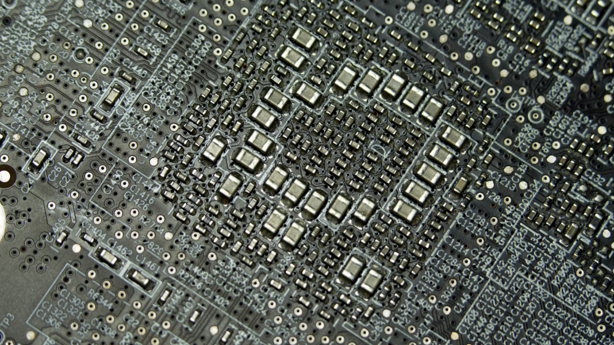
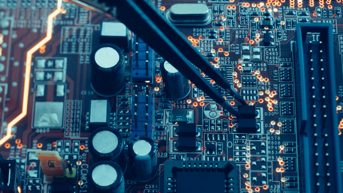
First, you should know that there are two ways to attach a component to a circuit board: the surface mount method, or SMD, and the Through Hole technique. In the surface mount technology, you have copper pads on the board, and you have to lay the components on top of them. 

You then have a through-hole technique where you stick the ends of a component through the board and then solder them from the bottom. If you are new to PCBs and not skilled at soldering, the through-hole technique is the way to go. However, the components tend to be bigger, so you will not be able to create a compact design. 

Below, we will discuss the step-by-step PCB assembly process on a large scale. 

Soldering 

The assembly process starts with soldering to the circuit board. The machine carries out an inspection at the start, in which it inspects the circuit board and ensures it is aligned. Once it is aligned, the machine will apply solder across the board’s surface evenly and smoothly. The machine ensures that the solder comes in contact with all the pads.  

Pick and Place Machine

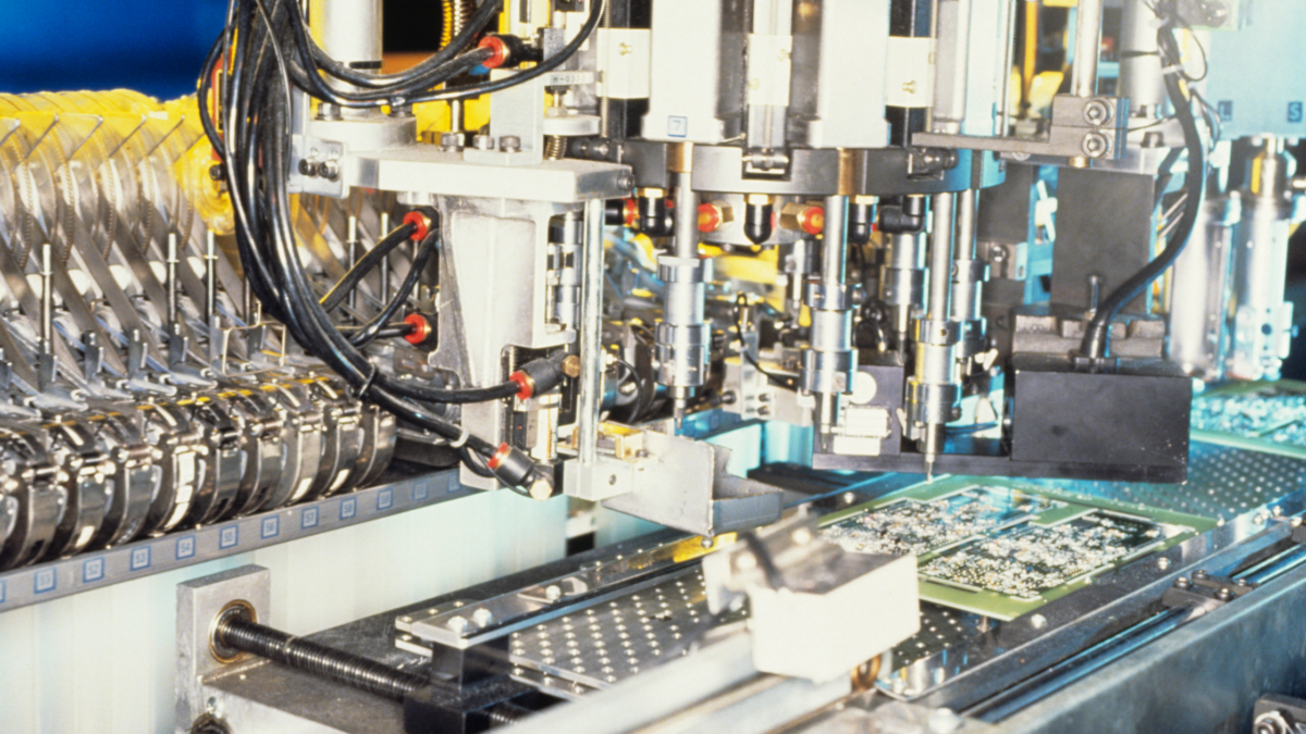
After soldering, the next assembly step requires the board to go to the pick-and-place machine. You must use a manual process for a low-volume prototype assembly, so you must place the board inside annually. The pick-and-place machine select’s it’s tools and then collects individual parts to place them on the board for rapid succession. After the pick and place process, the board is ready to refloat. 

The head that moves back and forth on this machine can hold eight components simultaneously. The parts that come from reels include the tape and reel board. The head travels and picks up over eight parts at a time from the reels and advances them so that the next part is ready. 

Refloat Process 

Refloat process is crucial because the solder needs to melt for adherence. This will make the board good for both mechanical and electrical connections for all the parts. It travels across the big machine and comes out from the other side after being cooked. Once the solder cools, junctions between each part come into creation. 

To Conclude

After the surface mount assembly, you can install through-hole components and create beta appliances. As you can see, manufacturing a printed circuit board involves a step-by-step process and careful considerations. The assembly process can, however, vary according to the size of the board and its electrical components.

As you can see, the PCB manufacturing process requires state of the art machinery and qualified expertise. If you want your printed circuit board assembly to be highly efficient and functional, you should look for a good manufacturer. Expert manufacturing companies are thorough with their design and assembly process, and can pave way for excellent appliances thanks to their sleek design. 

Why is Metal Core PCB Important?

Metal Core PCB are composed from copper film used for circuit lithography, a metal layer with a high heat dissipation capacity, and a dielectric layer. Copper and aluminiumare the materials most frequently used to fabricate metal layers. However, manufacturers also use stainless steel sometimes. Copper outperforms aluminium in terms of performance and electrical characteristics, but copper is more expensive.

The metal layer can be 100% metal or partly fibreglass (FR-4). Due to its high manufacturing complexity, the multilayer version of metallic PCBs is less prevalent. Instead, they can be single or double-sided. A multilayer MCPCB requires that the layers be distributed equally concerning the inner metal layer; for instance, a PCB with 12 layers would place the metal layer in the middle of the stack-up, with 6 layers above and 6 layers below.

Benefits of Metal Core PCB

Metal PCBs provide superior capacitive coupling, strong electromagnetic shielding, increased power density, and efficient thermal dissipation. Thermal vias, which are used in conventional PCBs, can further enhance thermal performance. Here are the top benefits of Metal Core PCB:

  • Thermal Dissipation

One PCB alternative with a higher heat conductivity is metal core PCB. They avoid potential circuit damage, increase power levels, and manage high-density circuits by keeping the heat as far away from the power components as feasible. Aluminium is a popular material for metal core PCB because it is affordable, recyclable, and has good electrical qualities. Moreover, metal core PCBs are incredibly faster than standard PCB.

The dielectric layer should be thin to establish the simplest path with the metal plate, and it typically has a thickness of about 0.003 to 0.006 inches. For instance, a test on a metal core PCB using integrated 1W LED revealed that its temperature stayed very near 25°C. However, the same power LED installed on a PCB attained a temperature 12°C higher than 25°C.

  • Better Stability and Strength

The rapid LED technology’s growth has highlighted concerns about heat dissipation. Particularly high-power LED lights and the circuit may have reliability and stability issues because these LEDs are typically positioned directly on the PCB. Heat dissipation can impair the operation of electronics that use a lot of power if the proper technique is not used. 

This issue is successfully resolved using metal PCBs. Aluminum adds resistance and strength to the PCB without adding weight and ensures longevity.

  • Dimensional Stability

As external circumstances change, metal core PCB’s size will remain more stable than one made of more conventional material, such as FR-4. PCBs containing metal layers have had a relatively slight size variation, between 2.5% and 3.0% when heated between 30°C to 150°C.

  • Longer Lifetime

Aluminium offers superior strength and longevity compared to materials such as fiberglass and ceramic, frequently used in producing PCBs. It consist of strong metal and reduces the risk of breakage during different production phases, while using finished products or assembly.

Conclusion

In contrast to ceramic substrates, the material architecture of metal core PCBs enables mounting configurations appropriate for solid-state relays in various control applications. A solid-state relay architecture requires a mechanically durable structure and thermally efficient, which metal core PCBs provide. 

Manufacturers are developing new forms of metal core PCB material, particularly dielectrics to achieve high thermal performance requirements that can even outperform current ceramic-based designs.

The Key Characteristics of the Surface Mount Technology: PCB Assembly

Surface Mount Technology or an SMT is a method of manufacturing circuit boards. The alternative to this would be through-hole circuit boards with different circuit board designs. Most circuit boards that you see in mobile phones today are a bunch of small chips placed on top of a circuit board panel.

Surface Mount Technology

A circuit board with surface mount technology will not necessarily have holes inside. Instead, they are on top of copper pads and copper traces on the circuit board. This surface mount technology is a semi-automated process that allows manufacturers to build all the different circuit boards in-house for various products.

With the help of this technology, manufacturers can easily mount electronic components on the surface of printed circuit boards. This mounting technique is very different from the insertion technique that manufacturers conventionally use with holes.

In other words, it is an alternative to the older practices of developing circuit boards with the help of through holes. Since it is a newer rendition, it overcomes many shortcomings of the through-hole technology on the surface mount.

SMD

One of the critical characteristics of the surface mount technology is an SMD, otherwise called a surface mount device. When you browse the markets, you will find multiple range packages of SMD. These packages vary in different sizes and shapes.

SMD Passive Components

A large portion of the SMD resistors are either capacitors or resistors. The package sizes of these passive components come in sizes standard pack. Other surface mount device components include crystals and coils.

Resistors and capacitors generally vary in dimensions, shapes, and sizes. Other forms of SMD components that you can find include diodes and transistors. These are often very small in regards to shape and size. They connect within a circuit board with the help of leads.

Approximately three leads are included within these packages. Identifying which way the device must shift can help with the manufacture of the printed circuit board.

Integrated Circuits

You will find that there is a variety of packages that come in handy for integrated circuits. The use of the package depends entirely on the amount of interconnectivity that the component needs. For instance, a logic chip is only installed with 14 to 16 pins. On the other hand, other processors and chips can come with about 200 or more.

Since requirements can vary so greatly, there are a number of different packages that you can find. Like the packages, the processes in the SMT process also differ from the conventional through-hole PCB method.

Solder Paste Printing

One of the most distinctive processes of the SMT method involves solder paste printing. This refers to the place where you need components. The printed circuit board usually comes with a very fine and thin piece of metal.

On the circuit board, there are solder pads. In surface-mount technology, stencils and squeegees usually do the job of applying solder to the appropriate pads on the circuit board. This method of solder mask application is becoming very widely used and popular. This is especially the case in the subcontract sector.

To Conclude

As you can see, the surface mount technology has great significance today and is prevailing against the conventional through-hole method. The characteristics of the surface mount technology in the PCB manufacturing industry, along with its large-scale implementation are speeding up the manufacture of electrical appliances and technology. This, in turn is accelerating the world towards a prosperous future.


How is PCB Made in China?

Circuit boards are the heart of just about any piece of electronic item that you use. China is responsible for a big chunk of the world’s circuit board production. In hindsight, printed circuit boards are a specific assembled product, even though they may look very complicated. The United States have largely relied on China for PCB production, but there seems to be a re-shoring trend underway.

The Re-Shoring Trend

Re-shoring is the act of having production units that were outsourced at foreign locations back to your hometown. US PCB companies have been setting up production units back to their hometowns and shutting down operations in other countries. The reason for this move is the increasing amount of labor costs in other countries, paired with the prevailing supply chain issues that are slowing down delivery times.

Not only that, due to the Geopolitical tensions, US citizens now demand that the products they consume are natively built. There is also a threat of intellectual theft when you hand over technical operations to other countries. Taking all of these existing factors into account, the re-shoring trend has become evident.

Below, you can get a glance of the technical process.

The Very First Step

Before a design file can be put into production, engineers will first glance at the file to ensure there are no inconsistencies within the design. Engineers need to check things such as trace gaps, files, drills, and other aspects of the digital PCB design they receive. This will ensure that the engineer did not design the PCB in a way that you cannot manufacture it.

Printing the Design onto Film

Once the design is reviewed and corrected, the design will then turn into films. You can make films and use light to project an image onto a board with a photoresist. This is similar to how you would expose a photograph. Once you have the design, you need to transfer it onto a copper board blank. Before you can shift the film onto the blank board, manufacturers will first prepare the board.

Board Production

The PCB board is manufactured using a layer of fiberglass in between and then gluing copper on the outside. In a large-scale manufacturing unit, large sheets of blank PCB boards are cut down into smaller components. After the board is cut, it is sent to the drilling unit. There are two reasons manufacturers drill a printed circuit board.

The first is to connect the components, and the other is to accommodate the wire holes connecting the copper layers. To begin with the drilling process, an operator will take an MDF board as exit material.

They will then attach an aluminum sheet on top of the board, which acts as an entry for the machine drill. This machine is fully automated, allowing it to select the right size of the drill. After doing so, it loads it into the drill head.

Most PCB manufacturing units in China will use highly optimized drills that can rotate up to 15 thousand revolutions per minute. After that, the corners are trimmed to make them rounded, and the surface is cleaned. Then, the machine automatically smoothens the edges of the board.

Final Steps

The steps that follow allow the board to go through a series of processes where copper is plated, and a printer prints photosensitive film to the copper board. Once the film is attached, further mechanical processes and solder masking will lead to the completion of the printed circuit board.

The solder mask protects that copper surface. The attachment of the components and testing is done with the help of machines. After the testing is complete, workers will separate all individual PCBs from the large production panel.


How to Repair Broken Traces on a Circuit Board?

Different methods can help you repair broken traces from a circuit board. Today, there is a prevailing shortage of microchips that are microprocessors. Traces are what connect microchips and all other essential components on a circuit board.

Damages on Traces

Traces on a circuit board are not new to damage. They can suffer from damage in several ways. They can get damaged due to accidents or even due to dirt or residue. Most of the time, damage on the PCB traces is due to corrosion. Corrosion can happen because there is a leak in the electrolytic capacitor or a leak in the batteries. They can also be caused due to poor storage. To repair broken or damaged traces on a circuit board, you will first need certain tools and equipment.

What will you need?

To start with, you are going to need a soldering iron. Remember that your soldering iron does not have to be the best in the market. However, it is recommended that you have a soldering station rather than just one soldering iron. Along with that, you will need a high-quality gel flex and a very good set of precision tweezers.

You will need a blade, scalpel, or sharp object for cleaning, and a UV solder mask, along with solder, for reapplication. Do not forget that you will also need some wire for the actual trace repair. Afterward, you will need some isopropyl alcohol and some q-tips, cotton buds, and a toothbrush.

It is also very good to have multimeter so that you can keep a check on your work progress. Not to mention, a multimeter will be beneficial because it helps you keep a check on your work to make sure you’ve renewed continuity in the damaged traces.

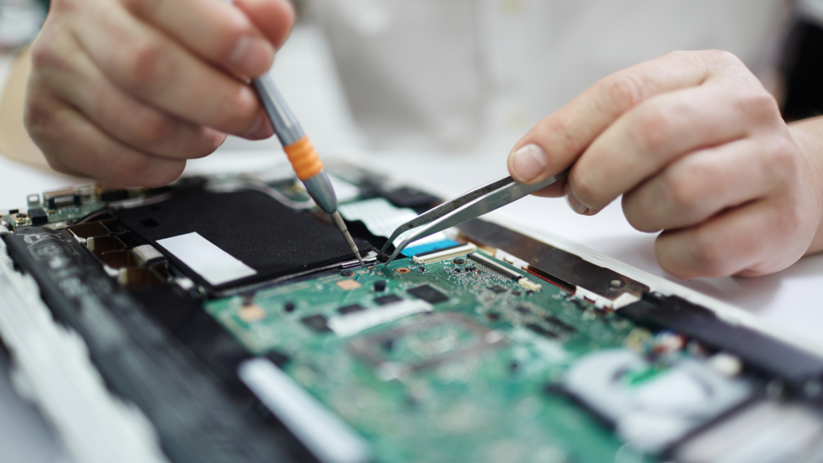
Other things you’ll need include very sharp eyesight and a steady pair of hands. If you don’t have good eyesight, it is always a good choice to use a microscope. A microscope is an effective way to se what you’re doing without making errors.

You can even connect a camera to this microscope to enhance your work. Since a microscope can be pricey, they are not easily available. In this situation, a magnifier is a better alternative when trying to repair broken traces on a printed circuit board.

Use Enameled Wire

You should use enameled wire, the same type of wire you would use on a transformer or an electromagnet. It has an enameled coating, which means that it is insulated, making it very functional inside a printed circuit board. Nonetheless, this enameled coating comes off very easily with the heat of the soldering iron.

So if you need to run a trace over the board where it might come in contact with other metal, the insulation will stop it from creating a short. As you can see, repairing broken traces on a printed circuit board requires extensive consideration and thought, and you must be willing to take all the precautions to do a clean job.

To Conclude

With careful consideration and some knowledge of printed board repair, you can easily repair the broken traces on a printed circuit board. The above-mentioned types of equipment can help make the repairing process easier. All you have to do is spot the broken trace, clean the corrosion, and apply new wires on them with the help of solder.

Why Is The PCB Manufacturing Process So Essential?

When trying to understand how a printed circuit board works and its application, it’s essential to know the manufacturing process. Learning about the manufacturing process of PCBs can help you gain a more insightful understanding of the circuit board’s functioning. The manufacturing process for printed circuit boards introduces you to some of the most fundamental concepts of the PCB design.

Basic Board Structure

The PCB consists of multiple layers, and these layers also impact the manufacturing process. The critical layers of the printed circuit board include the copper layers. These are where you will find the traces. The traces are the wires within the circuit that connect the different components.

In a two-layered circuit board, you will have a top copper layer and a bottom copper layer. Between the two layers, you will find a dielectric material that is made of fiberglass. This fiberglass material is also called the Substrate, and engineers often refer to it as FR4.

In addition to that, most boards also contain a layer that sits on top of the copper, as well as on the bottom of it. This layer is called Soldermask, and it is a critical aspect of the PCB manufacturing process.

Soldermask

Soldermask is a layer of insulation that sits on top of the copper so that the components on the board are not in contact with each other. Very often, you can also find a layer of silkscreen on top of the printed circuit board. This silkscreen is text that allows you to identify the components inside a PCB.

The solder mask is the green layer of material that you find on PCBs. Whenever you have exposed copper on the PCB, you can apply a solder mask to it. The manufacturing process also involves making holes inside printed circuit boards, called through-holes.

These holes are plated through the board, with copper all the way through. These are the sorts of things that manufacturers will typically solder through. There are other types of holes, and engineers will call them Via.

Vias connect a wire on one layer to another layer. If you look at a board carefully, you will have lighter green areas and darker green areas. Where you have lighter green areas, you will find copper sitting on top of the FR4 Substrate.

Silkscreen

Copper on a printed circuit board is effectively on a large plane and traces. The silkscreen sits on top of the highest layer, which gives the reflection of the lighter colors on the board. Darker areas on the copper are simply solder mask and Substrate.

Manufacturing a Multilayered Board

In a multilayered board, what you have is a sandwich of individual boards. In other words, creating a multilayered board will require you to stack one board on top of another. A motherboard inside a computer can have about 16 layers which are very complex.

The Significance of the Process

The PCB process is incredibly complex. It encompasses multiple steps, and there are incredibly large boards with multiple different designs that are flowing through the factory. In today’s world, highly automated and large-scale machines make it possible to produce high volumes of Printed Circuit Board in a single day. This simple phenomenon has expanded the growth of technological innovations around the world, giving way to the acceleration of mechanical and electronic progress.

How did Circuit Board Assemblies Evolve?

All inventions go through evolutionary courses. PCBs, or printed circuit boards, went through an incredible course in history. If there is one thing that has challenged the electronic assembly industry, it is the need for miniaturization. As components inside an electrical unit get smaller and closer together, it pushes the printing and cleaning process to the edge. One may think that miniaturization is a product of the last 5-10 years. However, this process began about a hundred years ago.

History of Circuit Assemblies

When you think of circuit board assemblies, you instantly think of them as modern technology. It all started with Albert Hanson, a German scientist who filed a patent for a device that would improve telephone exchange boards. This primitive circuit board had wires attached to a conductive substrate and bonded to a flat surface.

This device consisted of technology that you would consider a precursor to the modern-day circuit board. It also had the simple through-hole design of today’s circuit board. The first real circuit board came patented in 1927 by American inventor Charles Ducas. His circuit board design had stenciled conductive materials on a wooden board that was flattened out.

This may be how the word, “board” is incorporated into what you now call a circuit board. Charles Ducus utilized a stencil to print the wires directly onto the board. He also applied ink for the conduction of electricity. This concept aligned the electronic path to an insulated surface, which created a more recognizable device as a printed circuit board today.

Evolution into Multi-Layered Circuit Board

Ducus conceptualized his invention further and thought of the possibility of layering multiple boards, which will give existence to a multi-layered circuit board. However, connecting multiple boards into a multi-layered object would require another great inventor who had the capabilities to turn his concept into a reality.

Then came Paul Eisler, who is widely known and appreciated for inventing today’s printed circuit board. After leaving Australia in the early days of World War 2, he settled in England. He worked in a newspaper printing company, which led him to use his printing expertise to formulate an idea that printed electronic circuits onto boards.

This was a giant leap forward in the labor-intensive practice of hand soldering each wire manually. His inventions helped in World War 2 because they were used in radio sets that the British and Americans used during the war.

Etching Design

In 1943, a patent was issued for a circuit board design that was more advanced than the one used in World War 2. It involved etching the circuits onto copper foil and on glass-reinforced non-conductive substrates. In 1948, the US Army released this technology to the public so that it could prompt widespread development of the innovation.

Transistors

In the 1950s, the printed circuit board became subject to further enhancement as transistors emerged. These components helped reduce the size of the electronics and made it easier to incorporate PCBs into electronics. This also improved the reliability of the electronics, and it started the beginning of the long-driven goal of miniaturization. In the 1950s and 60s, PCBs evolved into double-sided boards with identification printing on one side and electronic components on the other side.

Concluding Thoughts

Today, printed circuit board designs have zinc plates, silicon chips, solder masks, and more components that make electronic components more effective. Moreover, the circuit board assembly technology known as the surface mount technology dominates the PCB world. Surface Mount Components are soldered directly onto the board and have become industry standard.

PCB 101

Circuit boards, which also go by the names, printed circuit boards and PCBs, consist of various electrical components. Comprising insulated board materials along with dozens of electrical components, PCBs feature different technologies ranging from surface-mounted to interconnected systems. They’re made for specific electronic circuits and perform a specified or a set of different actions.

Since their early development during the 1900s, the laminate materials on PCBs have gone through various developments and technological advances. Charles Ducas was the first to submit a patent for his circuit. The idea was vividly defined as placing a pathway comprising electrical components directly over an insulated material board. But, the real development and use didn’t find ground until after World War II.

Typical Use and Purpose of Printed Circuit Boards

In today’s modern world, just about every device has a printed circuit board. Nearly all electronic devices around us have some type of PCB or a combination of them to function effectively. In simple words, PCB technology was a ground-breaking development that paved the way for massive technological advancements to take place on a global scale.

The PCB technology is powering a range of applications and equipment across multiple industries. It’s safe to say that without modern printed circuit board production, research, and development, it wouldn’t be possible for massive innovations to take place in our technological space. Here’re a few uses and PCB’s modes of deployment around us:

Aviation

Aviation utilizes high-performance and lightweight PCBs to operate and design aircraft. Considering the size of the size of a typical PCB, that’s a humungous role that the technology is serving at the moment. From communication and drone construction to guidance systems, PCB technology offers lightweight and functional solutions.

Automobile

The automobile industry uses PCBs in a rather spectacular manner. The use of PCB allows automobile brands and manufacturers to place safety sensors inside vehicles! From keyless entry to ignition systems, PCB enables a range of different features in different makes and models of vehicles around us. Besides, the latest computerization of vehicles has stirred up demand for more intelligent vehicles.

Home Automation

The home automation industry is also utilizing PCB technology to assist in different features and other technologies. If you live in a home with a surveillance system, smart thermostats, and smart appliances, just about all of these technologies will have PCBs.

Entertainment

The entertainment industry probably has one of the biggest innovations that mankind has ever seen, thanks to PCB technology. It’s the development of flat-screen televisions. Humankind would’ve been stuck on fat monitors and TVs if PCBs didn’t replace the tube technology and wiring that was used previously. Even the miniature MP3 pods you may have used comprised of tiny PCBs that enable music playback and audio recording with wide variations.

Lastly, we don’t need to tell you what smartphones are, what they’re for, and how they’ve made our lives easier. However, it’s best to share that they comprise industry-best PCB technology to enable different functions and features that most users require regularly.

Latest Advances in the Technology

Here’s a list of some of the major advances in PCB technology, including fabrication techniques:

  • LDI, which stands for Laser Direct Imaging, is among the most precise ways to create PCB materials’ design images. It replaces the photochemical process that was too troublesome and usually inaccurate.
  • Flex PCBs technology allows greater flexibility in the fabrication of printed circuit boards. Thus, it’s easier to handle application-specific requirements when using PCBs in other technology-associated devices.
  • HDI stands for High-Density Interconnect Boards, is the main technology in use for efficient electrical component placement on insulated board material. It allows the placement of more components while requiring less space. Hence, it offers greater reliability and performance with reduced weight and space.

Conclusion

In the end, there’s a lot more to the PCB technology than just the recent developments and new fabrication techniques. Find out more through the latest research and studies to learn how PCB technology enabled a new era in modern technology.

Surface Mount Technology – What Is It All About?

Have you ever taken a look inside any of the modern electronic equipment in your house? Lots of commercially-produced electronic equipment doesn’t contain wire leads or other traditional components with inefficient integration. Now, critical electrical components of printed circuit boards are mounted on the board using a special integration and manufacturing process. Most components that are mounted on the printed circuit boards are minute in size, and that’s one of the major advantages of it.

In simple words, mounting minute and lightweight components on printed circuit boards to fulfill the same functions refer to Surface Mount Technology (SMT). Virtually speaking, nearly all electronic equipment of today comprises Surface Mount Technology.

Since it offers lightweight features with optimal functionality, it has become one of the most favorable choices of PCB across the industry. Here’s a quick overview of the SMT technology (or components) and its benefits.

Surface Mount Technology – Overview of Devices

Surface mount components are quite different from their leaded counterparts due to various advantages. Plus, they offer a range of features and durability that’s different from the traditional components. They are placed on the printed circuit boards and then soldered to them. In contrast, the traditional components are wired to the insulated material board.

To help you understand, the traditional components required a wire between every two components, whereas this doesn’t happen with SMT components in the latest PCBs. Also, there is solder inside the board holes for components rather than wiring for traditional leaded components. The packaging styles are different from various components using the surface mount technology. The three main categories of the packaging styles include integrated circuits, passive components, and transistors/diodes.

Biggest Advantages

In simple words, the three main reasons PCB manufacturers loved switching to the surface mount technology were speed, cost-effectiveness, and reliability. All these benefits become practical during the assembly process due to easier implementation and simplified manufacturing. SMT is a major step up from the traditional leaded components.

You must know that the development, design, and manufacture of new equipment and electronic circuits are also positively impacted by the wide range of benefits from SMT components. Fortunately, designers and manufacturers of PCBs have come up with more advantages of the said tech than disadvantages.

Reduced Power Ratings

It’s worth mentioning that through the application of it in printed circuit boards, the power ratings of the components have dropped. We will take a surface mount resistor as a practical example for discussing the reduced power ratings of the said technology.

For your information, a standard leaded resistor is capable of dissipating nearly 0.25 watts while its counterpart, i.e., SMT component, dissipates quite less. However, if you’re someone working with SMT components, make sure you check the manufacturer’s data before purchase.

Efficient and Denser Circuits (Lightweight and Smaller)

The trend for smaller volumes but increased functionality has been realized to a certain extent with the help of components. The miniaturization of critical components in PCBs has improved the lightweight features and enabled circuits to be denser.

Conclusion

SMT components power a range of different circuit boards, including Printed Circuit Boards (PCBs). It’s easy to use and solder them onto circuit boards. However, they require adequate care due to the chances of extensive damage. The components offer a faster, lighter, and more durable alternative to the traditional leaded components in printed circuit boards. Plus, it’s worth mentioning that the use of SMT components in PCBs has enabled manufacturers and designers to make huge cost-saves.

Defining PCBs in New Light

Printed Circuit Boards or PCBs have evolved to become much more complex than before. Considering the early patenting and development, modern functionalities of devices featuring PCBs have improved to make them more intelligent. Initially, they had limited functionalities, so there was room for further research and development. Today, PCBs are miniature and enable a range of functionalities. Modern PCBs hardly resemble their predecessors from the early 1900s. Through multi-layered programming and complex system enhancement, the latest PCBs have transformed our technological space.

Do you realize how significant the presence of FPGAs and HDI was a decade ago? They were once found only in the most expensive designs and fabrications but are now readily available almost everywhere. Here’s what to know about the latest developments and the bright future of the constantly improving PCBs industry.

Innovation with Board Cameras

Board cameras, or, more popularly, “PCB cameras,” refer to circuit board-mounted cameras. They have an aperture, image sensor, and lens to help with digital video and image capture. Through the lens, PCB cameras allow moderate-quality visually captured information to be transmitted to the main device’s storage. These cameras are only around the size of a quarter but can easily mount a PCB of any size. Thanks to recent innovations, modern circuitry and PCB development allow the installation of these small cameras into nearly any type of electronic device with full functionality and capability.

The primary areas of development in regard to PCB cameras were video and photo imaging and capture. However, those were the early phases, and the improvements are taking place on a greater scale. While being miniature, the PCB-mounted board cameras can take high-resolution videos and images with consistency. They can be a powerful solution worldwide for many industries involving electronics and more.

Development of PCB Autoplacers

The latest PCBs present in electronic devices that we use and see today contain an autorouter inside their design. The autorouter is an electrical component of the printed circuit boards and helps make the automation process easier. The said component on a PCB helps reroute electronic functions across the board to enhance and model the PCB layout’s characteristics. This results in an easier automation process. But, the real hurdle is that it takes a lot of labor and time to create, set up, and utilize the abilities of autorouters inside PCBs.

Overall, the faster automation process offers no value since it compensates for the time wasted in creating and setting up the autorouter component. But, with the use of autoplacers, the industry is seeing several changes. Multiple PCB designers and manufacturers now find autoplacers as suitable alternatives. The latter enhances the integration of electrical and mechanical CAD systems while also speeding the manufacturing process through simplification. Although they offer viable benefits, they aren’t widely accepted across the industry. The primary reason for that lies in the difference between the constraints of autoplacers and autorouters.

High-Speed Features Following Latest PCB Fabrication

People are now demanding faster electronics to perform functions and tasks such as production, manufacturing, and processing more efficiently. This is possible thanks to the latest PCB developments’ high-speed features. Manufacturers and designers keep working on new and fresh concepts to come up with unique ideas that help the industry fulfill all consumers’ demands. Since electronics largely rely on speed and PCB efficiency.

It’s critical that designers now turn their attention to the widespread adoption of high-speed PCBs. From analog PCBs to digital PCBs, designers find high-speed PCBs a unique subject for discussion.

Conclusion

There’s no end to the improvement and developments that can take place in the PCBs industry. After all, that’s how some of the major industries and businesses are powered. For your information, the technological advances and improvements have provided a better outlook on the upcoming changes in the tech space.