
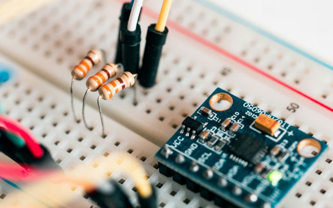
For the IoT industry, PCBs are the unsung heroes who create functional connections in IoT devices. As the building block of electronic devices, PCBs play an important role in fostering IoT technologies’ efficiency, performance, and reliability. This thin board is made of insulating material with conductive copper track, allowing electronic components to route their connectivity for a circuit.
However, this building block comes with its own set of challenges that we will address so that you can see why your IoT device is acting up. Although these challenges can be a huge hindrance for us, they come with their solutions and an opportunity for us to learn and grow.
Challenges Faced by PCBs in IoT Devices
As IoT aims to connect and network devices, it is on OCB designs to mold how they work.
Size Constraints and Miniaturization
Printed circuit boards (PCBs) face a formidable challenge in IoT due to the devices’ ever-shrinking size requirements. As IoT applications demand increasingly compact and portable solutions, PCBs must grapple with the intricacies of miniaturization. This section explores the impact of size constraints on PCB design, examining the trade-offs between functionality and space efficiency. Strategies such as multi-layered PCBs and surface mount technology will be discussed to address the miniaturization challenge in IoT devices.
Power Consumption Issues
Efficient power management is critical in IoT devices where prolonged battery life and energy conservation are paramount. PCBs face the challenge of optimizing power distribution, minimizing energy loss, and ensuring overall energy efficiency. This segment delves into the intricacies of power consumption challenges, exploring how advanced power delivery systems, low-power components, and intelligent design can mitigate power constraints’ impact on PCBs in IoT applications.
Environmental Factors and Durability
IoT devices often operate in diverse and demanding environments, ranging from extreme temperatures to high humidity or corrosive conditions. PCBs must contend with maintaining functionality and structural integrity under such varied circumstances. This section explores the impact of environmental factors on PCB performance, delving into materials engineering, protective coatings, and design considerations that enhance the durability of PCBs in IoT devices.
Solutions to PCB Challenges in IoT Devices
With these solutions, it is prominent that IoT devices are revolutionizing PCBs’ basic structure and design.
Advanced Manufacturing Techniques
The implementation of advanced manufacturing techniques becomes crucial to address the challenges posed by size constraints and the need for miniaturization in PCBs for IoT devices. This section explores cutting-edge methods such as additive manufacturing, HDI (High-Density Interconnect) technology, and precision assembly processes. By adopting these approaches, engineers can optimize space utilization, enhance component integration, and overcome the limitations associated with the physical dimensions of IoT devices.
Energy-Efficient Design Strategies
Efficient power consumption is a cornerstone in the successful operation of IoT devices. PCBs play a pivotal role in achieving energy efficiency. This segment delves into design strategies that minimize power consumption without compromising performance. Topics include utilizing low-power components, smart power management systems, and implementing energy harvesting technologies. IoT devices can extend battery life and reduce their environmental impact by adopting these energy-efficient design principles.
Materials Innovation for Durability
PCBs must be robustly durable to ensure the longevity of IoT devices. This section explores innovative materials and coating technologies that enhance PCB resilience. A detailed examination of material science solutions will be provided, from corrosion-resistant materials to protective coatings that shield against harsh environmental conditions. By integrating these advancements, PCBs can withstand the rigors of varied environments, ensuring the reliability and durability of IoT devices.
As we delve into these solutions, it becomes evident that the evolution of PCB technology is intricately linked to overcoming the challenges posed by IoT requirements. Integrating advanced manufacturing techniques, energy-efficient designs, and innovative materials is paving the way for more resilient and high-performing PCBs in the rapidly expanding landscape of Internet of Things applications.
Wrapping Up
As we go through these challenges and their recurring solutions, we tend to address the designers’ perspective and also what IoT industries face. On the other hand, this era of innovation demands more user-friendly PCBs so that they can easily be integrated into the devices.
Recent Comments