
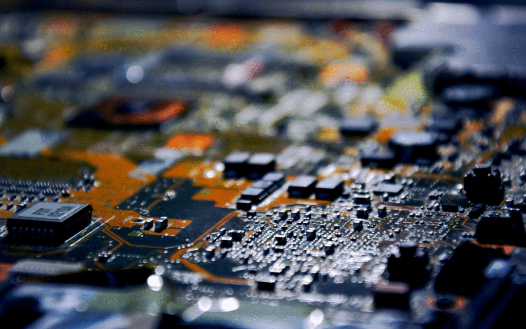
Printed Circuit Boards (PCBs) are at the heart of nearly every modern electronic device, from smartphones and medical equipment to industrial machinery and automotive systems. Understanding the PCB manufacturing process is crucial for engineers, product developers, and businesses seeking reliable electronic solutions. At Nova, we specialize in delivering high-quality PCBs with precision, consistency, and speed. Our team ensures your products meet the highest performance standards.
In this guide, we’ll break down each stage of the PCB manufacturing process, highlight why it’s so essential, and explain why Nova is a trusted partner for companies across industries.
What Is the PCB Manufacturing Process?
The PCB manufacturing process is the series of steps required to design, assemble, and test a printed circuit board. It transforms raw materials like copper, fiberglass, and solder mask into the complex green boards that power electronic devices. This process is not just about attaching components; it’s about ensuring precise connectivity, structural integrity, and long-term reliability.
PCBs typically consist of multiple layers, including:
-
Copper Layers: Carry electrical signals through traces.
-
Dielectric Layer (FR4 Substrate): Provides insulation and mechanical strength.
-
Solder Mask: Insulates copper traces and prevents short circuits.
-
Silkscreen: Adds identifiers, labels, and component markings for assembly and troubleshooting.
Each layer and step in manufacturing impacts the board’s durability and performance. Whether creating simple two-layer boards or complex 16-layer designs, Nova follows stringent quality standards throughout the entire process.
Why the PCB Manufacturing Process Matters
A well-executed PCB manufacturing process ensures:
-
Precision Connectivity: Traces and vias must align perfectly to prevent electrical failures.
-
Durability: Quality materials and proper soldering extend the board’s lifespan.
-
Safety: Consistent inspection prevents defects that could damage end products.
-
Scalability: Reliable processes allow seamless scaling from prototypes to mass production.
By mastering each stage, Nova helps clients avoid costly rework, speed up time-to-market, and maintain consistent product quality.
Step-by-Step: The PCB Manufacturing Process
1. PCB Design and Layout
The process begins with a carefully engineered design. Using CAD software, Nova’s team creates a schematic and layout that defines component placement, trace routing, and layer configuration. The design stage considers signal integrity, thermal management, and manufacturability to ensure efficient assembly.
2. Solder Paste Application
Before components are added, a thin layer of solder paste is applied to the pads where components will be mounted. Using a stencil and precise machinery, Nova ensures paste is applied only where needed — preventing shorts and guaranteeing strong connections later in the process.
3. Pick and Place Assembly
Next comes the pick and place step. Automated machines accurately position components onto the PCB according to the design layout. This high-speed, high-precision process minimizes human error and ensures consistent quality, even for boards with hundreds of components.
4. Soldering (Reflow or Wave)
After placement, components must be permanently attached to the board:
-
Reflow Soldering: Common in surface-mount technology (SMT). Boards pass through a controlled oven where heat melts solder paste, securing components in place.
-
Wave Soldering: Used for through-hole components. Boards pass over a “wave” of molten solder to attach components in bulk.
Nova selects the appropriate soldering method based on the board’s design and component mix.
5. Layering and Multilayer Stack-Up
For multilayer PCBs, multiple copper and substrate layers are laminated together. This “sandwich” structure increases board density and allows for more complex circuits. Nova’s advanced lamination techniques ensure alignment and minimize signal interference between layers.
6. Solder Mask and Silkscreen Application
The solder mask (usually green) is applied to insulate copper traces and prevent accidental bridges during soldering. The silkscreen is then printed to label components, test points, and logos, making the board easier to assemble and troubleshoot later.
7. Drilling and Plating (Vias and Through-Holes)
Holes are drilled into the PCB for vias (connections between layers) and through-hole components. These holes are plated with copper to create conductive pathways, ensuring signals travel between layers without loss.
8. Inspection and Quality Control
Quality assurance is critical. Nova employs:
-
Automated Optical Inspection (AOI): Detects misaligned components, soldering defects, and incorrect placements.
-
X-Ray Inspection: Identifies hidden flaws beneath components like BGAs.
-
Manual Inspection: Performed by skilled technicians for final verification.
9. Electrical Testing
Before delivery, every PCB undergoes functional testing to ensure it meets design specifications. Continuity tests check for open circuits, while in-circuit tests confirm component performance and alignment.
10. Feedback and Continuous Improvement
Nova integrates feedback from testing and client requirements into future production runs. This commitment to continuous improvement ensures every board meets or exceeds industry standards.
Materials in the PCB Manufacturing Process
A quality PCB depends on premium materials. Nova uses:
-
FR4 Fiberglass Substrate: Provides strength and insulation.
-
Copper Foil: Conducts electrical signals.
-
High-Temperature Solder Mask: Prevents shorts and improves durability.
-
Lead-Free Solder: Meets RoHS compliance for eco-friendly electronics.
Nova’s Commitment to Excellence in PCB Manufacturing
Nova isn’t just another PCB supplier — we’re a full-service PCB manufacturer dedicated to precision, reliability, and customer satisfaction. Our manufacturing process is ISO-compliant, highly automated, and adaptable to custom requirements. Whether you need prototypes or large-scale production, we deliver consistent results tailored to your project’s demands.
Key benefits of choosing Nova:
-
Decades of Expertise: Proven experience in multiple industries.
-
Cutting-Edge Equipment: Ensures speed and accuracy at every stage.
-
Rigorous Quality Control: From raw materials to final testing.
-
Custom Solutions: Flexible designs to meet your specific needs.
Why Partner with Nova for Your PCB Manufacturing Process?
When selecting a PCB partner, quality and reliability matter most. Nova’s meticulous PCB manufacturing process ensures:
-
Shorter lead times without compromising quality.
-
Seamless transition from design to production.
-
Reduced errors and improved yield rates.
-
Comprehensive testing for guaranteed performance.
Our customer-focused approach means we collaborate closely with your team, providing insights at every stage of development to ensure your product succeeds.
Ensuring Quality Through Every Step
The PCB manufacturing process is the backbone of modern electronics. Each step, from design and soldering to inspection and testing, impacts performance, safety, and longevity. By choosing Nova, you gain a trusted partner dedicated to precision engineering and dependable manufacturing. Whether you’re developing consumer electronics, industrial systems, or specialized equipment, our expertise ensures your PCBs meet the highest standards.
Recent Comments