How to Choose the Right PCB Design Software for Your Project

Selecting the best PCB design software is a critical step in ensuring the success of your PCB board design projects. Whether you’re a seasoned professional or just starting, choosing the right software can streamline your workflow, enhance design accuracy, and ultimately produce superior results. This comprehensive guide will help you navigate the selection process by focusing on your project requirements, budget, and skill level, with relevant internal and external resources linked throughout.

1. Assess Your Project Requirements

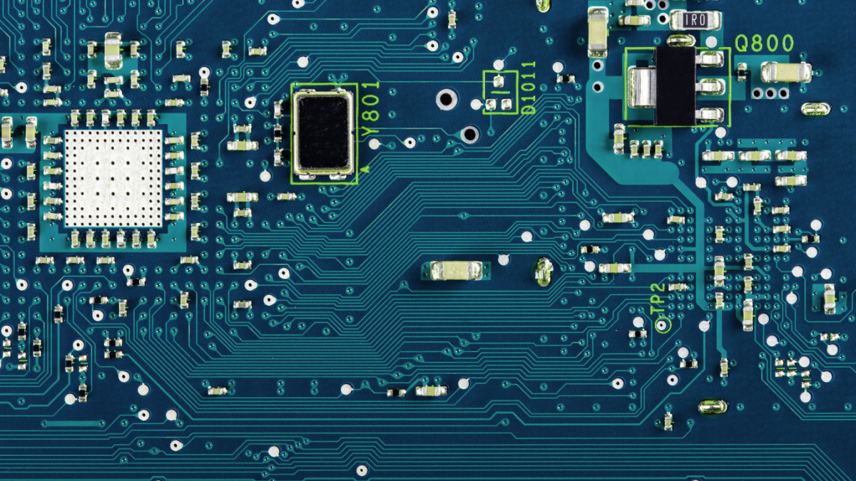
  • Complexity and Scale: The complexity of your PCB design dictates the level of software you need. For intricate, multi-layer designs, advanced features such as signal integrity analysis and thermal management are essential. Altium Designer is a software that excels in handling complex PCB board design projects. For simpler designs, KiCad might suffice.blue pcb software design
  • Specific Design Rules: Your software should support the specific design rules required for your project, such as spacing constraints, impedance control, and more. Ensuring that your PCB design software aligns with your project’s unique requirements can prevent costly revisions later. For more detailed considerations, refer to our article on Avoiding Common PCB Design Mistakes.

2. Budget Considerations

  • Free vs. Paid Software: Depending on your budget and the complexity of your project, you may choose between free tools like EasyEDA and paid options such as Cadence Allegro. Free software is great for hobbyists or small-scale projects, but for more demanding tasks, investing in professional-grade software is often worth it.
  • Subscription vs. Perpetual Licensing: Consider how long you’ll need the software. Subscription-based models might be more affordable for short-term projects, while perpetual licenses can be more cost-effective for ongoing use. For insights on how we manage different projects within budget, visit our Project Management page.

3. Skill Level and Learning Curve

  • Ease of Use: Beginners might prefer user-friendly software with a gentle learning curve, such as EAGLE, which offers extensive tutorials and a strong user community. As your skills develop, transitioning to more advanced tools like OrCAD can open up more sophisticated design possibilities. Explore our PCB Assembly page to see how we handle the transition from design to production.
  • Support and Community Resources: The availability of robust support and an active user community can significantly ease the learning curve. Software with extensive online resources, such as forums, video tutorials, and user manuals, can help you quickly overcome challenges. Our article on PCB Layout Tips offers practical advice that complements the tools you choose.

4. Key Software Features
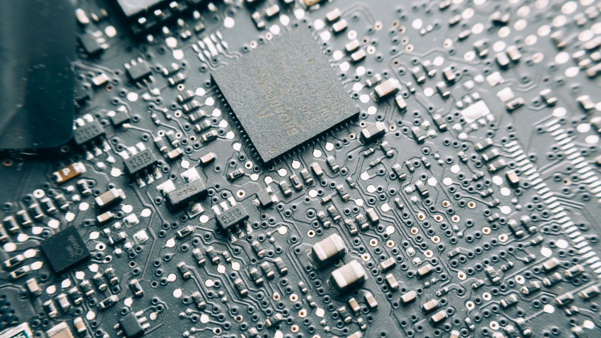
  • green pcb design softwareSimulation and Testing Capabilities: Reliable simulation and testing features are essential for verifying that your PCB design will function as intended before moving to production. OrCAD is known for its powerful simulation tools, which are crucial for identifying potential issues early in the design process. To learn more about how we ensure quality in every project, check out our Quality Assurance page.
  • Component Libraries and Third-Party Integration: Access to a comprehensive component library can streamline the design process. Tools like DipTrace offer extensive libraries and easy integration with third-party components, ensuring that you have all the necessary elements at your fingertips. This can be particularly helpful when working on projects that require specialized components.

5. Integration and Collaboration Tools

  • File Compatibility: Ensure that the PCB board design software you choose can handle the file formats your manufacturing partners use. Compatibility with industry-standard formats like Gerber files is non-negotiable for seamless production. For more on how we integrate design and manufacturing, visit our Manufacturing Services page.
  • Collaboration Features: If you’re working with a team, consider software that includes collaboration tools. Cloud-based platforms like Altium Designer allow multiple designers to work on the same project simultaneously, making it easier to manage complex projects. This feature is especially valuable when coordinating between design and production teams.

6. Try Before You Buy
green pcb board design

  • Free Trials and Demos: Before committing to a particular PCB design software, take advantage of free trials and demos to ensure it meets your needs. This hands-on experience is crucial for evaluating usability and features, ensuring that the software you choose is the best fit for your project.
  • Future-Proof Your Choice: Consider how your needs might evolve over time. If you plan to take on more complex projects or scale your operations, choose software that can grow with you. Altium Designer, for instance, offers a range of advanced features that can accommodate increasingly sophisticated designs, making it one of the best PCB design software options for professionals looking to future-proof their capabilities.

Choosing the right PCB design software is a pivotal decision that can influence the success of your projects. By thoroughly evaluating your project requirements, budget, and skill level, you can make an informed choice that ensures a smooth and efficient design process. Check out our PCB Services page for more on how we handle complex designs.
6 Ways to Reduce PCB Assembly Cost Without Sacrificing Quality

Reducing PCB assembly cost does not have to mean choosing the cheapest parts or cutting corners on quality. In many cases, the decisions made before a board reaches production have the greatest impact on the overall cost of a project. Component selection, documentation, design complexity, sourcing strategy, and production planning can all affect how efficiently a PCB moves from prototype to finished assembly.

For product teams and OEMs, the goal should be to eliminate avoidable expenses while maintaining the performance and reliability the application requires. A thoughtful approach can help control costs, reduce delays, and create a smoother path from initial build to larger production volumes.

1. Review the Design for Manufacturability

One of the best ways to manage PCB assembly cost is to identify potential manufacturing issues before production begins. Design for Manufacturability, or DFM, reviews can help uncover concerns involving pad dimensions, component rotation, spacing, and other details that may affect production.

Catching these issues early can help prevent unnecessary rework, delays, or design revisions later in the process. At Nova Engineering, we use DFM methods during prototype assembly to help customers transition more efficiently from prototype to production.

2. Build Flexibility Into Component Selection

In today’s electronics manufacturing environment, reducing PCB assembly cost is less about simply finding multiple suppliers and more about building flexibility into component selection from the start. When appropriate, identifying approved alternates can help manufacturers respond to supply chain changes without delaying production or compromising the design.

A flexible bill of materials can help reduce the impact of:

  • Long component lead times
  • Obsolescence or limited availability
  • Unexpected pricing changes
  • Dependence on a single source

Any substitute still needs to meet the electrical, mechanical, and performance requirements of the design. The lowest-priced component is not always the best choice if it creates reliability issues, qualification delays, or the need for an expensive redesign.

3. Choose the Right Component Sourcing Model

How parts are purchased can significantly influence PCB assembly cost and project management. Some businesses prefer to supply every component themselves, while others want their production partner to manage procurement.

Nova offers three sourcing approaches:

  1. Turnkey assembly: Nova orders and receives the required components.
  2. Consigned assembly: The customer supplies the components.
  3. Partially consigned assembly: The customer supplies certain parts while Nova sources the rest.

Choosing the right model can reduce procurement work and make better use of components a company already has available.

4. Match Production Planning to the Project Stage

A prototype and a mature production run should not always be approached the same way. Early builds are often focused on validating the design and identifying improvements, while established products may offer more opportunities to optimize purchasing and production efficiency. Planning around the actual project stage can help control PCB assembly cost without forcing production decisions too early. Nova supports prototype through high-volume assembly and operates a dedicated prototype line, allowing different projects to be approached according to their production needs.

Panelization can also influence efficiency, but there is no universal configuration that works for every board. Working with the manufacturer before finalizing panel requirements can help ensure the layout is appropriate for the board design and assembly process.

5. Provide Accurate, Complete Documentation

Manufacturing delays are not always caused by the assembly line. Incomplete, outdated, or conflicting project files can create questions before production even begins.

An accurate BOM, fabrication data, pick-and-place files, assembly drawings, and clear revision information can help prevent mistakes. Keeping documentation organized is a simple but important way to reduce avoidable PCB assembly cost and keep production moving.

6. Look Beyond the Lowest Initial Quote

The lowest price per board does not always represent the lowest total PCB assembly cost. Rework, communication problems, incorrect parts, production delays, and quality issues can add expenses that were not reflected in the original quote.

An experienced production partner can help identify potential issues early and provide the appropriate sourcing and production approach for the project. Nova Engineering provides turnkey, consigned, partially consigned, prototype, and production PCB assembly services, giving customers flexibility as their manufacturing needs change.

Build Cost Efficiency Into the Process

The most effective way to manage PCB assembly cost is to consider the entire manufacturing process rather than focusing on a single expense. Better documentation, flexible sourcing, early DFM review, and realistic production planning can all help reduce unnecessary costs while protecting quality.

By addressing these factors early, companies can build a more efficient manufacturing strategy and avoid expensive surprises as a project moves from prototype into production.

Surface Mount PCB Assembly vs. Electromechanical Assembly: What’s the Difference?

When designing and manufacturing electronic products, choosing the right assembly process is just as important as selecting the right components. Surface mount PCB assembly is the most common method used in today’s electronics, but it is not the only option. Many products also require electromechanical assembly, or even a combination of both processes, depending on their design and application.

Understanding how these assembly methods differ can help engineers, OEMs, and product designers determine the best manufacturing approach for performance, reliability, and cost. Companies like Nova Engineering provide both PCB and electromechanical services, allowing customers to streamline production under one manufacturing partner.

What Is Surface Mount PCB Assembly?

It is the process of placing electronic components directly onto the surface of a printed circuit board (PCB). Unlike traditional through-hole assembly, components do not require leads to pass through drilled holes in the board. Instead, automated pick-and-place equipment positions components with high precision before they are permanently soldered using a reflow oven.

Today, this process is the industry standard for most electronic products because it supports:

  • Higher component density
  • Faster automated production
  • Smaller and lighter PCB designs
  • Improved manufacturing consistency

From medical devices and telecommunications equipment to aerospace and industrial controls, surface mount technology enables manufacturers to produce compact, high-performance electronics.

What Is Electromechanical Assembly?

While surface mount PCB assembly focuses on assembling electronic components onto a circuit board, electromechanical assembly goes several steps further. It combines completed circuit boards with mechanical and electrical hardware to create a finished product or subsystem.

Electromechanical assemblies may include:

  • Wire harnesses and cable assemblies
  • Connectors and switches
  • Enclosures and chassis
  • Fans, motors, or power supplies

Rather than producing only the PCB, manufacturers integrate multiple components into a complete assembly that is ready for installation or final product integration.

Key Differences Between the Two

Although the two processes often work together, they serve different purposes throughout manufacturing.

Surface mount PCB assembly is centered on building the electronic circuit itself. It involves placing resistors, capacitors, integrated circuits, and other electronic components directly onto the PCB with automated equipment.

Electromechanical focuses on integrating that completed PCB into a larger mechanical system. This process often includes wiring, cable routing, fastening hardware, connectors, and functional testing to ensure every subsystem operates together correctly.

In many modern products, both assembly methods are used during different stages of production.

When Is Each Process the Best Choice?

For most modern electronics, surface mount PCB assembly offers the greatest advantages. Automated production allows manufacturers to place thousands of components quickly while maintaining excellent accuracy and repeatability. This makes it ideal for medium- and high-volume production, as well as compact electronic designs.

Electromechanical assembly becomes important when the finished product requires additional hardware or mechanical integration beyond the PCB itself. Industries such as aerospace, defense, medical equipment, telecommunications, and industrial automation often require both services.

Choosing the right process depends on several factors, including:

  1. Product complexity
  2. Environmental requirements
  3. Production volume
  4. Mechanical integration needs

Working with an experienced manufacturing partner helps determine the most efficient production strategy for each project.

Why Many Products Use Both

Rather than viewing these processes as competing options, manufacturers increasingly use them together. A circuit board may first go through surface mount PCB assembly, followed by electromechanical assembly that adds wiring, enclosures, connectors, and final system integration.

Nova Engineering supports this complete manufacturing workflow by providing prototype and production PCB assembly, mixed technology assembly, electromechanical assembly, inspection, testing, and box-build capabilities. Keeping these services under one roof can improve communication, shorten lead times, and simplify quality control throughout production.

Choosing the Right Manufacturing Solution

Surface mount PCB assembly has become the preferred method for building today’s compact, high-performance electronic circuits because it offers speed, precision, and efficient use of board space. Electromechanical assembly complements that process by transforming completed circuit boards into fully integrated products that are ready for real-world use.

By understanding the strengths of each manufacturing method, companies can choose the right combination for their application. Whether a project requires advanced PCB assembly, complete electromechanical integration, or both, selecting an experienced manufacturing partner helps ensure reliable performance from prototype through production.

Surface Mount Technology: What It Means for Modern PCB Assembly

Surface mount technology has become one of the most important methods used in modern printed circuit board assembly. Instead of inserting component leads through drilled holes, this process allows electronic components to be placed directly onto the surface of a PCB and soldered in place. This helps manufacturers build smaller, lighter, and more efficient boards for today’s electronics.

For companies like Nova Engineering, this process supports the precision, speed, and flexibility required for both prototype and production PCB assembly. Nova offers surface mount and mixed technology, helping customers bring reliable electronic products from concept to completion.

What Is Surface Mount Technology?

Surface mount technology, often called SMT, is a process that uses surface mount devices, or SMDs. These components are designed to sit on solder pads on the board rather than pass through holes like traditional through-hole components.

This difference matters because electronic products continue to become smaller, faster, and more advanced. SMT makes it possible to place many components in a compact space while still supporting strong electrical performance. It is commonly used in consumer electronics, medical devices, telecommunications equipment, industrial systems, and other applications where reliability and space efficiency matter.

How the SMT Assembly Process Works

The surface mount technology process is highly precise and typically uses automated equipment. While each project can vary depending on board design and production requirements, the basic process usually includes:

  1. Solder paste is applied to the PCB using a stencil.
  2. Automated pick-and-place equipment positions components on the board.
  3. The board passes through a reflow oven, where solder melts and forms connections.
  4. The finished assembly is inspected for placement accuracy, solder quality, and defects.

Inspection is especially important because SMT components are often very small. Nova uses automated optical inspection, along with detailed quality checks, to help confirm that assemblies meet performance expectations.

Why SMT Is So Widely Used

One of the biggest advantages of surface mount technology is efficiency. Because the process can be automated, it supports faster assemblies and more consistent placement than many manual methods. This is useful for higher-volume production, but it also helps improve repeatability for smaller runs and prototypes.

Another advantage is board density. SMT allows components to be placed closer together, and in many designs, parts can be mounted on both sides of the PCB. That gives engineers more flexibility when designing compact electronics.

SMT can also reduce weight. Since surface mount components are generally smaller than through-hole components, the finished board can be lighter and better suited for portable or space-conscious products.

SMT vs. Through-Hole Assembly

Although SMT is common, through-hole assembly still has an important place in PCB manufacturing. Through-hole components are inserted through drilled holes and soldered on the opposite side of the board. This can provide stronger mechanical connections, which may be useful for connectors, switches, or components that experience physical stress.

Many modern boards use a combination of both methods. This is known as mixed technology assembly. Nova supports surface mount and mixed technology, which allows customers to use the best assembly method for each component and application.

Important Considerations for SMT Components

While surface mount technology offers many benefits, it also requires careful planning. Component size, pad layout, solder paste application, heat exposure, and inspection standards all affect the final assembly.

Smaller parts can improve board density, but they also demand tighter process control. Poor placement, insufficient solder, excess solder, or misaligned components can lead to performance issues. That is why experienced assembly, accurate equipment, and reliable inspection systems are so important.

Why Precision Matters 

A well-built PCB depends on more than the technology used. It depends on how carefully that technology is applied. With surface mount technology, even a small placement error can affect the function of the entire board.

Nova Engineering brings decades of experience to prototype and production PCB assembly. For industries that depend on accurate, reliable electronics, quality assembly is essential. Every board must be built with the right process, the right inspection steps, and the right attention to detail.

Building Better Boards 

Surface mount technology has changed how modern circuit boards are designed and assembled. It supports smaller products, faster production, higher component density, and reliable performance when handled with the right process controls.

For businesses that need dependable PCB assembly, SMT is not just a manufacturing method. It is a practical way to support the advanced electronics people rely on every day.

How Components on a Circuit Board Work Together to Power Modern Electronics

Have you ever thought about how much we rely on electronics every single day? From smartphones to industrial equipment, nearly everything we use depends on components on a circuit board working together seamlessly. Without these carefully designed systems, even the simplest device would not function.

At the core of modern electronics is the printed circuit board, often referred to as a PCB. It is not just a flat surface with parts attached. It is a precisely engineered platform where components interact to control power, process signals, and keep devices running efficiently. Understanding how these components work together helps highlight why quality PCB assembly matters, especially for companies like Nova Engineering that focus on reliability and precision.

Why Each Component Matters

Every PCB is designed with a purpose, and each element plays a specific role. When one piece fails, it can affect the performance of the entire system. That is why properly selected and assembled components on a circuit board are critical for long-term functionality.

Let’s break down some of the most important components and how they contribute to a working circuit.

Resistors: Controlling Electrical Flow

Resistors are one of the most common components on a circuit board. Their job is simple but essential. They regulate the flow of electrical current and help maintain safe voltage levels across the system.

Without resistors, circuits could easily overload, leading to overheating or permanent damage. They ensure that each part of the board receives the correct amount of power, which is especially important in sensitive electronics.

Capacitors: Storing and Releasing Energy

Capacitors act like temporary energy storage units. Among the key components, they store electrical energy and release it when needed.

They help stabilize voltage, filter noise, and support consistent performance. You will find capacitors in almost every electronic device, from consumer products to complex industrial systems.

Inductors: Managing Current and Magnetic Energy

Inductors are another type of passive component that plays a key role in managing electrical flow. These components on a circuit board store energy in a magnetic field when current passes through them.

They are commonly used in power supplies and filtering applications. Inductors help smooth out fluctuations in current and work closely with capacitors to maintain steady operation in circuits.

Transistors: Switching and Amplifying Signals

Transistors are among the most critical components on a circuit board because they act as both switches and amplifiers. They control the flow of electrical signals and allow circuits to perform complex tasks.

There are two primary types used in modern electronics:

  • Field Effect Transistors (FET)
  • Bipolar Junction Transistors (BJT)

These small but powerful components are essential for processing signals in everything from computers to communication devices.

Diodes: Directing Electrical Flow

Diodes ensure that electricity flows in only one direction. They protect circuits from damage caused by reverse current.

They are commonly used in power conversion, signal demodulation, and protection circuits. Without diodes, many electronic systems would be far less stable and reliable.

How It All Comes Together

While each part has its own role, the true power of a PCB comes from how all the components on a circuit board work together. Resistors regulate current, capacitors stabilize voltage, inductors manage energy flow, transistors process signals, and diodes control direction.

This level of coordination requires careful design and precise assembly. That is where experienced manufacturers like Nova Engineering make a difference. By ensuring that every component is correctly placed and properly integrated, they help create circuit boards that perform reliably in real-world applications.

The Bigger Picture for Modern Electronics

From everyday consumer devices to advanced industrial systems, the performance of electronics depends on the quality of the components on a circuit board and how well they are assembled. Even the smallest detail can impact overall functionality.

As technology continues to evolve, the demand for high-quality PCB assembly will only grow. Understanding how these components work together not only builds appreciation for modern electronics but also highlights the importance of choosing the right manufacturing partner.

PCB Troubleshooting: Common Assembly Issues and How to Catch Them Early

PCB troubleshooting is an important part of building reliable electronics. Even a well-designed board can run into assembly-related problems if materials, placement, soldering, or inspection steps are not carefully managed. In 2026, as boards continue to become smaller, denser, and more complex, it is less about guessing and more about following a consistent process that identifies issues early.

For manufacturers and product teams, the goal of pcb troubleshooting is not just to fix a bad board after the fact. It is to understand what caused the issue, prevent it from repeating, and keep production moving with confidence. That matters whether you are building a prototype, preparing for a new product introduction, or scaling into production.

Start With the Most Common Problem Areas

Many assembly issues can be traced back to a few core areas. Solder defects remain one of the most common reasons boards fail inspection or testing. These can include insufficient solder, solder bridges, cold joints, tombstoning, or poor wetting. Component placement problems are also common, especially on high-density boards where alignment tolerance is tight.

Another major area in pcb troubleshooting is materials verification. Incorrect parts, outdated components, polarity mistakes, and kit inconsistencies can all create avoidable failures. In some cases, the board itself is not the problem at all. The issue may come from the bill of materials, design file mismatch, or an error introduced before the board ever reached the line.

Use a Step-by-Step PCB Troubleshooting Process

Effective pcb troubleshooting works best when it follows a clear sequence instead of jumping straight to repair. A practical process often looks like this:

1. Review the documentation

Start by checking the Gerber files, BOM, assembly drawings, and revision level. Small file mismatches can create larger downstream issues.

2. Inspect the board visually

Look for missing parts, wrong orientation, solder bridges, lifted pads, or obvious handling damage.

3. Verify materials and placement

Confirm that the correct components were used and placed in the right locations.

4. Check solder quality

Review joints for consistency, coverage, and possible defects that could affect conductivity or reliability.

5. Run electrical or functional testing

If the board looks acceptable but still fails, test continuity, isolation, and real-world function to narrow down the issue.

6. Trace the root cause

Strong pcb troubleshooting does not stop at identifying the symptom. It asks why the defect happened and what process should change to prevent repeat failures.

Inspection Technology Matters More Than Ever

Modern pcb troubleshooting depends heavily on inspection systems and process control. Automated Optical Inspection, or AOI, is especially useful for catching placement and solder issues that may be easy to miss during manual review. Functional testing and final verification are also critical when boards are headed into demanding applications.

This is one reason manufacturers are placing more value on structured quality systems in 2026. As assemblies grow more compact and performance expectations rise, troubleshooting becomes faster and more reliable when it is backed by documented inspection procedures, trained staff, and repeatable workflows. Nova highlights automated SMT inspection, 100% final visual inspection, and in-house engineering support as part of its assembly process.

Why Prevention Is a Big Part 

The best pcb troubleshooting efforts begin before assembly starts. Design for Manufacturability review can uncover pad sizing issues, rotation problems, and other layout concerns that may create defects later in production. Material planning, kit verification, and inspection checkpoints also reduce the chance of rework and delays.

For companies moving from prototype to larger production volumes, this approach can make a major difference. Catching issues early helps reduce scrap, protect schedules, and improve long-term product reliability. That is especially important in industries where consistency matters, such as medical, aerospace, military, telecommunications, and industrial electronics.

Building Better Boards From the Start

It is not just about repairing defects. It is about creating a smarter assembly process that supports quality from the first build onward. When manufacturers combine careful documentation review, strong inspection methods, and root-cause analysis, they put themselves in a better position to deliver dependable boards with fewer surprises.

For teams that need support from prototype through production, working with an experienced assembly partner can make pcb troubleshooting more efficient and far less reactive. Nova Engineering’s focus on prototype, turnkey, consigned, and partially consigned PCB assembly reflects the kind of process-driven support that helps customers move forward with greater confidence.

Quality Control of Printed Circuit Boards in Modern Electronics

The quality control of printed circuit boards is one of the most critical factors in producing reliable, high-performing electronic devices. From consumer electronics to medical equipment and industrial systems, printed circuit boards (PCBs) serve as the foundation for functionality. As designs become more compact and complex in 2026 and beyond, manufacturers rely on rigorous quality control to ensure boards perform exactly as intended—every time.

This article explains what quality control of printed circuit boards involves, why it matters, and how modern inspection and testing methods help prevent failures before products ever reach the field.

What Is It?

Quality control of printed circuit boards refers to a structured set of inspections, tests, and verification steps used throughout the PCB manufacturing and assembly process. These checks ensure that materials, components, solder joints, and electrical connections meet defined performance and reliability standards.

Unlike basic visual checks used in the past, today’s quality control of printed circuit boards relies on automation, data tracking, and industry standards to catch defects early—before they turn into costly failures.

Why Quality Control Matters in PCB Manufacturing

The importance has grown significantly as electronics have become smaller, faster, and more interconnected. Even a minor defect—such as a solder bridge, missing component, or micro-crack—can lead to intermittent failures that are difficult to diagnose later.

Key reasons quality control is essential include:

Ensuring Long-Term Reliability

Devices are expected to operate consistently over long lifespans, often in harsh environments. Proper quality control of printed circuit boards helps confirm that electrical connections are sound and components function as designed under stress.

Reducing Manufacturing Costs

Identifying defects early reduces rework, scrap, and warranty claims. In 2026, manufacturers increasingly focus on “right-first-time” production, where strong quality control lowers total production costs.

Supporting Regulatory and Industry Compliance

Many PCBs must comply with standards such as IPC-A-610, RoHS, REACH, and ISO-based quality systems. Quality control of printed circuit boards ensures compliance and helps manufacturers avoid costly delays or penalties.

Protecting Brand Reputation

Consistently high-quality PCBs translate directly into reliable end products. This builds trust with customers and strengthens long-term brand credibility.

Key Stages: Quality Control of Printed Circuit Boards

Incoming Material Inspection

Before assembly begins, components and bare boards are inspected to verify authenticity, correct specifications, and physical condition. This step is increasingly important due to global supply chain variability and counterfeit risks.

In-Process Inspection

During assembly, boards are inspected at multiple stages to catch issues as they happen. Common in-process quality control methods include:

  • Automated Optical Inspection (AOI) to detect placement and solder defects

  • X-ray inspection for hidden joints such as BGAs and QFNs

  • Solder paste inspection (SPI) to ensure accurate paste deposition

These steps allow manufacturers to correct issues before they compound.

quality control of printed circuit boards- Nova

Electrical and Functional Testing

This also includes electrical testing to verify continuity, isolation, and signal integrity. Functional testing confirms that the assembled board performs as expected in real-world operating conditions.

Final Verification

Before shipment, boards undergo a final quality review to confirm they meet all design, performance, and documentation requirements. This ensures consistency across production runs.

Building Confidence Through Consistent Quality

Strong quality control of printed circuit boards is not just a manufacturing requirement—it’s a strategic advantage. When implemented correctly, it ensures product reliability, reduces long-term costs, and supports compliance in a demanding regulatory environment.

By investing in thorough inspection, testing, and process control, manufacturers can deliver printed circuit boards that perform reliably across applications and industries—meeting the expectations of both customers and the technologies they rely on. At Nova Engineering, this commitment to quality control is built into every stage of PCB assembly, helping ensure consistent performance from prototype through production.

When to Outsource Printed Circuit Board Assembly

Understanding when to outsource printed circuit board assembly is critical in today’s fast-paced electronics industry. As product designs become more complex and demand fluctuates, many companies are rethinking whether to keep PCB assembly in-house or partner with a trusted contract manufacturer.

Outsourcing isn’t just about reducing costs—it’s about aligning your capabilities with your strategic goals. Done right, it enables faster production, fewer quality issues, and a more agile response to changing market needs.

The High Cost of In-House Assembly

Building and maintaining an in-house assembly line requires substantial investment. From specialized equipment like pick-and-place machines and reflow ovens to ongoing technician training and quality assurance systems, the operational burden is high. This infrastructure also needs to evolve alongside rapid changes in PCB technology.

One of the clearest signs of when to outsource printed circuit board assembly is when these costs begin to outweigh the value of keeping production internal. Contract manufacturers like Nova Engineering have already made those investments—and they spread them across multiple clients, lowering the cost per unit. Outsourcing lets you tap into that infrastructure without having to build it yourself.

Indicators It’s Time to Consider Outsourcing

There’s no one-size-fits-all answer to when to outsource printed circuit board assembly, but several signs can indicate it’s time to shift to an external partner:

  • Increased lead times due to resource limitations or equipment bottlenecks 
  • Inconsistent quality or higher failure rates on delivered boards 
  • Delayed product launches from stretched internal teams 
  • Difficulty sourcing components or keeping up with inspection requirements 
  • Frequent demand fluctuations that strain production planning 

If any of these sound familiar, outsourcing can relieve pressure and improve output reliability.

Benefits of Contract Manufacturing Partnerships

Understanding when to outsource printed circuit board assembly is key to unlocking the advantages of a reliable contract manufacturing relationship. Partnering with a trusted PCB assembly provider opens the door to specialized capabilities that might not exist in-house. Contract manufacturers are constantly upgrading their tools, certifications, and knowledge to meet industry demands—from aerospace to medical and automotive applications.

When you outsource to an experienced manufacturer, you gain access to:

  • Advanced manufacturing techniques like fine-pitch BGA placement or HDI 
  • Cleanroom and ESD-controlled environments for sensitive electronics 
  • Dedicated quality control systems, including AOI, X-ray, and functional testing 
  • Knowledge of regulatory compliance, such as IPC-A-610, ISO 9001, and RoHS 

These advantages are especially valuable when you’re scaling up, launching a new product, or handling complex board designs that require consistent precision.

Preserving Internal Focus and Speed

One of the most overlooked benefits of outsourcing is that it lets your engineering and product teams stay focused. Knowing when to outsource printed circuit board assembly can help ensure internal resources aren’t tied up solving manufacturing issues, which often delays development timelines.

By outsourcing PCB assembly, you free up key personnel to do what they do best—designing, testing, and iterating on new innovations. This clearer focus can accelerate development cycles and reduce time to market—an increasingly valuable advantage in competitive product categories.

Building in Flexibility for Growth

As demand changes, so should your production strategy. Rigid in-house operations often struggle to keep pace with variable order sizes, evolving product specs, or sudden market shifts. Knowing when to outsource printed circuit board assembly helps you build flexibility into your business model.

Contract manufacturers can adapt quickly to changing volumes or requirements. Whether you’re producing hundreds or tens of thousands of boards, they offer scalable capacity without the need for internal investment or delays.

A Strategic Move Toward Smarter Manufacturing

Outsourcing printed circuit board assembly isn’t a shortcut—it’s a strategic choice that allows companies to grow more efficiently. Knowing when to outsource printed circuit board assembly matters most when your team is spread too thin, production costs are rising, or your technology is falling behind, and it’s time to evaluate your options.

A qualified contract manufacturer like Nova Engineering can help you lower risk, maintain high quality, and speed up delivery—while your team stays focused on innovation. For many companies, that’s the difference between staying competitive and falling behind.

6 Educational Circuit Board Facts That Power Modern Electronics

From the smartphone in your pocket to the industrial systems that run factories, circuit boards are at the heart of nearly all electronic technology. Yet most people know surprisingly little about what makes these boards work—or why they’re so important. Here are six essential circuit board facts that offer insight into the design, functionality, and innovation behind today’s printed circuit boards (PCBs).

1. Circuit Boards Simplify Complex Electrical Systems

One of the most important circuit board facts is that PCBs reduce the need for bulky wiring. Before PCBs, electronics were assembled using point-to-point wiring, which was not only messy but also prone to human error and difficult to replicate at scale. Printed circuit boards replaced this with pre-designed copper traces, streamlining the design, reducing manufacturing errors, and making mass production of electronics feasible.

PCBs serve as both the physical structure and the electrical connection platform for components such as resistors, capacitors, diodes, and microchips—all neatly arranged on a single board.

2. There Are Several Types of PCB Configurations

Another essential entry in circuit board facts: not all PCBs are the same. The type of circuit board used depends on the application’s complexity and requirements. Common types include:

  • Single-layer PCBs – Ideal for simple electronics like calculators and LED lights

  • Double-layer PCBs – Used in more advanced consumer electronics

  • Multilayer PCBs – Found in servers, industrial equipment, and advanced computing

  • Rigid-flex PCBs – Used in aerospace, medical, and compact consumer devices

Each type supports specific performance needs, cost levels, and design constraints.

3. PCBs Can Have Over 50 Layers

One of the more surprising facts is that advanced PCBs can consist of more than 50 layers of copper and insulating material. These multilayer boards are essential for devices that require high-speed data transmission, complex signal routing, or power distribution across multiple channels.

High-performance computers, 5G infrastructure, and aerospace systems rely on these densely packed boards to maintain reliability and speed without increasing the device size.

4. Surface Mount Technology Has Replaced Older Techniques

Decades ago, through-hole technology was the standard for mounting components on a PCB. Today, Surface Mount Technology (SMT) is the dominant method. SMT allows components to be mounted directly onto the surface of the board, enabling:

  • Smaller board sizes

  • Faster automated assembly

  • Higher component density

This evolution in assembly methods is one of the most important circuit board facts influencing modern electronics design.

5. Circuit Boards Are Designed Using Specialized Software

Designing a circuit board isn’t done by hand—it requires precision software tools. Engineers use computer-aided design (CAD) programs like Altium Designer, Eagle, or KiCad to lay out the copper traces, component placement, and via locations. These tools generate Gerber files, which are the standard file format used by manufacturers to fabricate PCBs.

This digital design-to-manufacturing workflow ensures every printed circuit board meets exact specifications and performance requirements.

6. Clean Manufacturing Matters More Than You Think

One of the lesser-known but critical circuit board facts is how important cleanliness is during manufacturing. Dust, oils, or static discharge can compromise conductivity or damage sensitive components. That’s why PCB manufacturing facilities often follow strict environmental controls, similar to cleanrooms used in semiconductor fabrication.

Maintaining a controlled environment ensures higher reliability, longer board life, and reduced failure rates—especially in high-stakes industries like medical, military, or aviation.

Why These Circuit Board Facts Matter

Understanding these circuit board facts helps demystify the technology that powers modern life. Whether you’re designing consumer electronics, industrial systems, or mission-critical devices, knowing how PCBs function—and how they’re evolving—helps you make smarter design, sourcing, and manufacturing decisions.

At Nova Engineering, we specialize in assembling reliable, high-performance circuit boards for a wide range of industries. From prototype to production, we ensure every layer, connection, and component is built with precision and care.

Why are Circuit Board Assemblies Printed?

Before modern advancements in electronics, connecting components in a circuit was a manual and error-prone task. Engineers relied on point-to-point wiring to create circuits inside radios, computers, and early appliances. This method was time-consuming, difficult to repair, and prone to short circuits. Everything changed when the concept of a circuit board printed with conductive paths emerged.

The shift to printed circuit boards (PCBs) revolutionized electronic design and manufacturing. Instead of hand-wiring every connection, engineers could now design a board with etched copper traces to automatically route electricity between components. This innovation drastically improved efficiency, reliability, and scalability.circuit board printed- nova engineering

The Origins of Printed Circuit Boards

In 1936, Austrian engineer Paul Eisler introduced the first concept of a circuit board printed with copper pathways. He created a non-conductive base material with a printed copper circuit on top, which allowed components to be soldered onto predefined traces. While early versions looked nothing like today’s compact multilayer PCBs, the foundational idea remains the same.

The transition to printed technology laid the groundwork for the mass production of electronic devices. It also reduced human error and allowed for more precise circuit design, which is essential in everything from consumer electronics to aerospace systems.

How Is a Circuit Board Printed Today?

Modern PCB technology begins with a simple sheet of copper laminated onto a fiberglass-reinforced epoxy material (commonly FR4). The steps to manufacture a printed circuit board are precise and controlled to ensure quality and consistency.

1. Design and Gerber Files

The first step in creating a circuit board printed design is using computer-aided design (CAD) software. Engineers generate what’s known as Gerber files—digital blueprints that detail the layout of copper traces, pads, vias, and holes. These files drive every phase of manufacturing.

2. Drilling

Once the layout is finalized, the board undergoes a drilling process to create holes that will later hold through-hole components or vias. Each circuit board printed design includes precision-placed holes, created by computer-guided drills based on the Gerber file.

After drilling, the board is cleaned to remove any dust or debris, ensuring proper adhesion of materials in later steps.

3. Creating Copper Traces (Etching)

To create the conductive pathways, a photosensitive resist layer is applied to the copper surface. A light is used to expose only the desired circuit pattern. After exposure, the unprotected copper is removed using a chemical etching process, leaving behind the intricate network of copper traces.

This etching step is what transforms a blank copper sheet into a PCB with a custom circuit layout.

4. Solder Mask and Silkscreen

Once the traces are etched, a green (or sometimes blue, red, or black) solder mask is applied. This layer insulates the copper traces and prevents solder bridges between components during assembly.

The silkscreen layer is printed next. It provides labels, part numbers, and component identifiers directly on the circuit board printed surface, guiding technicians during assembly.

The Value of Printed Circuit Board Assemblies

A PCB with accuracy enables faster assembly, more compact device designs, and easier mass production. Whether used in smartphones or spacecraft, printed circuit boards provide the foundation for electrical functionality and performance.

Printing circuit boards also enables automation in the next stage: PCB assembly. Using automated pick-and-place machines, manufacturers can quickly place thousands of components onto a circuit board with pinpoint accuracy. Combined with reflow soldering and inspection, this results in highly reliable electronic systems.

The Role of Printing in Modern PCB Manufacturing

Today, the term printed circuit board refers not only to the physical traces on a PCB but also to the broader manufacturing process that allows for miniaturization and performance in advanced electronics. As devices become smaller and more powerful, printed circuit board technology evolves alongside them.

From its origins in early radios to powering high-speed computers, the innovation of having a circuit board printed with precise paths has transformed electronics forever. For engineers and manufacturers, it remains one of the most essential building blocks of any electronic design.