Types of PCB Assembly Processes: An In-Depth Guide

Printed circuit boards (PCBs) are the core of nearly every modern electronic device—from smartphones and laptops to medical equipment and industrial systems. But behind every functioning PCB is a carefully executed series of PCB assembly processes that bring the board to life.

If you’re wondering what these processes are and how they differ, this guide will walk you through the most common types of PCB assembly processes and explain when and why each is used.

What Is PCB Assembly?

Before diving into the types of PCB assembly processes, it’s important to understand what PCB assembly entails. PCB assembly (also known as PCBA) refers to the process of attaching electronic components to a blank printed circuit board using soldering techniques.

Without a reliable assembly process, even a perfectly designed board will fail to function. That’s why selecting the right method is key to performance, cost, and reliability.

Surface Mount Technology (SMT) Assembly

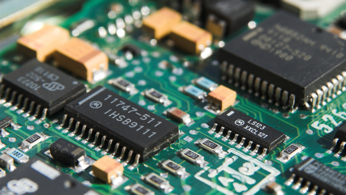
Surface Mount Technology (SMT) is the most widely used of all PCB assembly processes. It involves placing components directly onto the surface of the PCB using solder paste and a reflow oven.

Why choose SMT?

  • Compact and efficient for high-density designs

  • Faster and more cost-effective for large runs

  • Widely used in consumer electronics, medical devices, and more

SMT allows for high-speed automated assembly and is ideal for miniaturized components.

Through-Hole Assembly

Through-hole assembly is a traditional method where component leads are inserted through pre-drilled holes in the PCB and soldered on the opposite side. Though it’s been largely replaced by SMT, through-hole is still useful for components that require strong mechanical bonds.

Best for:

  • Connectors, transformers, and large capacitors

  • Industrial and high-power applications

  • Environments with high mechanical stress

While slower and more manual, through-hole remains valuable for certain durable designs.

Mixed Technology Assembly

Mixed technology combines SMT and through-hole components on a single PCB. This hybrid method is useful when certain parts aren’t available in surface-mount format or when specific performance needs call for both technologies.

Mixed assembly allows for:

  • Greater design flexibility

  • Improved cost-performance balance

  • Complex builds with unique component requirements

Many advanced industrial and aerospace products rely on this blended approach.

Rigid-Flex PCB Assembly

Rigid-flex PCBs combine rigid and flexible circuit layers into a single design. These processes are ideal for compact devices where space is limited and movement is required.

Applications include:

  • Wearable technology

  • Aerospace and defense systems

  • Medical imaging equipment

This approach reduces the need for connectors and cables, improving reliability and reducing size and weight.

Ball Grid Array (BGA) Assembly

Ball Grid Array (BGA) is a specialized surface-mount packaging used for microprocessors and other integrated circuits. Instead of edge pins, BGA components use tiny solder balls underneath the chip, increasing connection points and improving heat dissipation.

Advantages of BGA:

  • High pin density in a small footprint

  • Excellent thermal and electrical performance

  • Ideal for high-speed and high-power devices

BGA is commonly used in advanced computing and graphics systems.

Why PCB Assembly Processes Matter

Each of these processes serves a specific purpose, and the choice depends on the design complexity, performance requirements, and environment in which the final product will operate.

For compact consumer electronics, SMT is often the best choice. Industrial machinery might demand through-hole or mixed assemblies for added strength and reliability. Rigid-flex and BGA are essential in specialized applications where performance, size, and functionality must all align.

Choosing the Right Process for Success

Understanding the range of available PCB assembly processes allows engineers and designers to make better decisions during product development. The right process ensures not only a functioning product but also one that’s optimized for durability, efficiency, and cost.

At Nova Engineering, we specialize in high-quality PCB assembly using SMT, through-hole, and mixed technologies. With decades of experience and a focus on precision, we help clients build electronics that perform under pressure—no matter the industry or application.
Understanding the PCB Environmental Impact: What You Need to Know

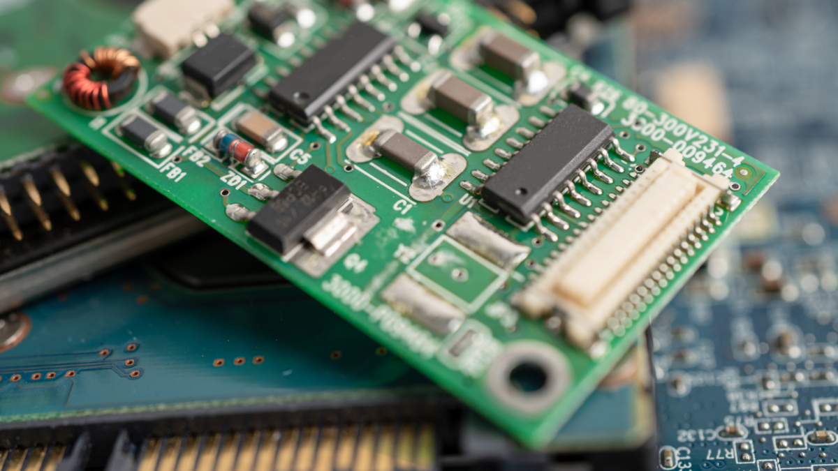
As electronics become more essential to daily life, so does the need to understand the pcb environmental impact. Printed circuit boards (PCBs) are foundational to nearly all electronic devices, but their production and disposal can have significant environmental consequences. From material sourcing to end-of-life management, each stage in the PCB lifecycle plays a role in shaping its ecological footprint.

This article explores how the PCB manufacturing process affects the environment and what the electronics industry is doing to minimize that impact.

Materials and Sourcing: The Environmental Cost of Raw Inputs

The environmental journey of a PCB begins with its materials. Substrates like FR-4, commonly used in board construction, are made from fiberglass-reinforced epoxy — a material that involves hazardous chemicals and energy-intensive manufacturing. While effective and durable, these traditional substrates contribute to environmental strain.

Copper is another key material. As the main conductor in PCBs, it’s essential for functionality but also requires significant mining and refining. These operations consume large amounts of energy and release emissions into the environment. Recycling copper is a more sustainable solution, helping reduce the pcb environmental impact by minimizing the need for new resource extraction.

Solder, once made predominantly with lead, has shifted toward lead-free alternatives to reduce toxicity. Even so, lead-free solders can contain other metals that require careful disposal and recycling procedures to prevent environmental harm.

Manufacturing: Energy and Emissions

Manufacturing PCBs consumes a notable amount of energy, particularly during high-temperature processes like reflow soldering. These ovens and other assembly equipment often rely on non-renewable electricity sources, further amplifying the pcb environmental impact.

Emissions are also a concern. Processes such as soldering and cleaning can release volatile organic compounds (VOCs) and other airborne pollutants. To reduce emissions and energy use, manufacturers are turning to:

  • Energy-efficient machines and production systems

  • Smarter ventilation and HVAC solutions

  • Renewable energy sources where available

These upgrades not only reduce carbon footprints but can also cut operational costs over time.

Waste and E-Waste: Managing Byproducts and Obsolescence

PCB production generates a range of waste, including trimmed materials, defective boards, and excess components. More concerning, however, is what happens when PCBs reach the end of their lifecycle. Improper disposal contributes to the growing global issue of e-waste, with toxic materials leaching into soil and groundwater.

Recycling is a key solution. Valuable metals such as gold, silver, and copper can be recovered from old boards. Many countries now regulate e-waste disposal, requiring manufacturers and consumers to participate in proper recycling programs. Additionally, designing PCBs for easy disassembly can significantly increase the effectiveness of recycling and reuse efforts while helping to reduce overall pcb environmental impact.

Chemicals and Contamination

The assembly process for PCBs involves a range of chemicals — from fluxes to cleaning agents — that can pose environmental risks. If mishandled, these substances may contaminate water sources or soil. Some also pose health risks to workers when not properly managed.

To counter this, many manufacturers are adopting:

  • Eco-friendly fluxes and solvents

  • Automated chemical handling systems

  • Compliance with environmental regulations such as RoHS and REACH

These strategies reduce pollution and improve worker safety without sacrificing quality or performance.

Transportation and Supply Chain Footprint

In today’s global supply chains, PCBs and their components often travel long distances before reaching their destination. This logistics process contributes to carbon emissions, especially when relying on air freight or diesel-powered vehicles.

Manufacturers are working to reduce this impact by consolidating shipments, choosing more local suppliers, and using electric or low-emission transport options. These efforts support a smaller pcb environmental impact while streamlining operations.

End-of-Life Responsibility and the Ongoing PCB Environmental Impact

The environmental footprint of a PCB doesn’t end at manufacturing. When electronic devices are discarded, their circuit boards often go with them. Without proper recycling, these materials may sit in landfills for decades, slowly leaching harmful substances.

End-of-life strategies are now a critical part of the electronics industry’s shift toward sustainability. Take-back programs, local recycling centers, and international regulations all aim to manage e-waste responsibly and reduce long-term pcb environmental impact. Manufacturers are also investing in design improvements that make disassembly and component reuse more efficient and cost-effective, supporting a circular economy approach in electronics production.

Building a Greener Electronics Industry

Reducing the pcb environmental impact requires a full-lifecycle approach — from sustainable material sourcing to energy-efficient manufacturing and responsible disposal. Manufacturers that embrace eco-friendly practices not only help protect the environment but also meet growing consumer and regulatory demands for sustainability.

As awareness grows, so does innovation. With ongoing efforts to design cleaner, smarter, and more recyclable PCBs, the electronics industry is actively working toward a more sustainable future — one component at a time. At Nova, we’re proud to contribute to that future by integrating sustainable materials, energy-conscious production methods, and responsible end-of-life strategies into every stage of our PCB manufacturing process.

Our PCB Manufacturing Process Explained

Printed Circuit Boards (PCBs) are at the heart of nearly every modern electronic device, from smartphones and medical equipment to industrial machinery and automotive systems. Understanding the PCB manufacturing process is crucial for engineers, product developers, and businesses seeking reliable electronic solutions. At Nova, we specialize in delivering high-quality PCBs with precision, consistency, and speed. Our team ensures your products meet the highest performance standards.

In this guide, we’ll break down each stage of the PCB manufacturing process, highlight why it’s so essential, and explain why Nova is a trusted partner for companies across industries.

What Is the PCB Manufacturing Process?

The PCB manufacturing process is the series of steps required to design, assemble, and test a printed circuit board. It transforms raw materials like copper, fiberglass, and solder mask into the complex green boards that power electronic devices. This process is not just about attaching components; it’s about ensuring precise connectivity, structural integrity, and long-term reliability.

PCBs typically consist of multiple layers, including:

  • Copper Layers: Carry electrical signals through traces.

  • Dielectric Layer (FR4 Substrate): Provides insulation and mechanical strength.

  • Solder Mask: Insulates copper traces and prevents short circuits.

  • Silkscreen: Adds identifiers, labels, and component markings for assembly and troubleshooting.

Each layer and step in manufacturing impacts the board’s durability and performance. Whether creating simple two-layer boards or complex 16-layer designs, Nova follows stringent quality standards throughout the entire process.

Why the PCB Manufacturing Process Matters

A well-executed PCB manufacturing process ensures:

  • Precision Connectivity: Traces and vias must align perfectly to prevent electrical failures.

  • Durability: Quality materials and proper soldering extend the board’s lifespan.

  • Safety: Consistent inspection prevents defects that could damage end products.

  • Scalability: Reliable processes allow seamless scaling from prototypes to mass production.

By mastering each stage, Nova helps clients avoid costly rework, speed up time-to-market, and maintain consistent product quality.

Step-by-Step: The PCB Manufacturing Process

1. PCB Design and Layout

The process begins with a carefully engineered design. Using CAD software, Nova’s team creates a schematic and layout that defines component placement, trace routing, and layer configuration. The design stage considers signal integrity, thermal management, and manufacturability to ensure efficient assembly.

2. Solder Paste Application

Before components are added, a thin layer of solder paste is applied to the pads where components will be mounted. Using a stencil and precise machinery, Nova ensures paste is applied only where needed — preventing shorts and guaranteeing strong connections later in the process.

3. Pick and Place Assembly

Next comes the pick and place step. Automated machines accurately position components onto the PCB according to the design layout. This high-speed, high-precision process minimizes human error and ensures consistent quality, even for boards with hundreds of components.

4. Soldering (Reflow or Wave)

After placement, components must be permanently attached to the board:

  • Reflow Soldering: Common in surface-mount technology (SMT). Boards pass through a controlled oven where heat melts solder paste, securing components in place.

  • Wave Soldering: Used for through-hole components. Boards pass over a “wave” of molten solder to attach components in bulk.

Nova selects the appropriate soldering method based on the board’s design and component mix.

5. Layering and Multilayer Stack-Up

For multilayer PCBs, multiple copper and substrate layers are laminated together. This “sandwich” structure increases board density and allows for more complex circuits. Nova’s advanced lamination techniques ensure alignment and minimize signal interference between layers.

6. Solder Mask and Silkscreen Application

The solder mask (usually green) is applied to insulate copper traces and prevent accidental bridges during soldering. The silkscreen is then printed to label components, test points, and logos, making the board easier to assemble and troubleshoot later.

7. Drilling and Plating (Vias and Through-Holes)

Holes are drilled into the PCB for vias (connections between layers) and through-hole components. These holes are plated with copper to create conductive pathways, ensuring signals travel between layers without loss.

8. Inspection and Quality Control

Quality assurance is critical. Nova employs:

  • Automated Optical Inspection (AOI): Detects misaligned components, soldering defects, and incorrect placements.

  • X-Ray Inspection: Identifies hidden flaws beneath components like BGAs.

  • Manual Inspection: Performed by skilled technicians for final verification.

9. Electrical Testing

Before delivery, every PCB undergoes functional testing to ensure it meets design specifications. Continuity tests check for open circuits, while in-circuit tests confirm component performance and alignment.

10. Feedback and Continuous Improvement

Nova integrates feedback from testing and client requirements into future production runs. This commitment to continuous improvement ensures every board meets or exceeds industry standards.

pcb manufacturing process

Materials in the PCB Manufacturing Process

A quality PCB depends on premium materials. Nova uses:

  • FR4 Fiberglass Substrate: Provides strength and insulation.

  • Copper Foil: Conducts electrical signals.

  • High-Temperature Solder Mask: Prevents shorts and improves durability.

  • Lead-Free Solder: Meets RoHS compliance for eco-friendly electronics.

Nova’s Commitment to Excellence in PCB Manufacturing

Nova isn’t just another PCB supplier — we’re a full-service PCB manufacturer dedicated to precision, reliability, and customer satisfaction. Our manufacturing process is ISO-compliant, highly automated, and adaptable to custom requirements. Whether you need prototypes or large-scale production, we deliver consistent results tailored to your project’s demands.

Key benefits of choosing Nova:

  • Decades of Expertise: Proven experience in multiple industries.

  • Cutting-Edge Equipment: Ensures speed and accuracy at every stage.

  • Rigorous Quality Control: From raw materials to final testing.

  • Custom Solutions: Flexible designs to meet your specific needs.

Why Partner with Nova for Your PCB Manufacturing Process?

When selecting a PCB partner, quality and reliability matter most. Nova’s meticulous PCB manufacturing process ensures:

  • Shorter lead times without compromising quality.

  • Seamless transition from design to production.

  • Reduced errors and improved yield rates.

  • Comprehensive testing for guaranteed performance.

Our customer-focused approach means we collaborate closely with your team, providing insights at every stage of development to ensure your product succeeds.

Ensuring Quality Through Every Step

The PCB manufacturing process is the backbone of modern electronics. Each step, from design and soldering to inspection and testing, impacts performance, safety, and longevity. By choosing Nova, you gain a trusted partner dedicated to precision engineering and dependable manufacturing. Whether you’re developing consumer electronics, industrial systems, or specialized equipment, our expertise ensures your PCBs meet the highest standards.

The History of Circuit Boards: From Invention to Innovation

The history of circuit boards is a fascinating journey through time, technology, and innovation. What began as a rudimentary method for connecting electrical circuits has evolved into a highly precise, miniaturized process that powers nearly every modern electronic device. At Nova Engineering, we specialize in high-quality PCB assembly in Denver, Colorado, and we take pride in the legacy that brought us to where we are today.

The Early Days: The First Concept of a Circuit Board

The history of circuit boards begins in the early 20th century with Albert Hanson, a German inventor who, in 1903, filed a patent for a method of constructing flat, layered circuits. While rudimentary, this early invention laid the groundwork for what we recognize today as the printed circuit board (PCB). Hanson’s design included conductive foil paths mounted to insulating boards, a clear precursor to today’s multi-layered systems.

In 1927, American inventor Charles Ducas advanced this idea by printing conductive paths directly onto a flat wooden board using stencil and conductive ink. His creation marked the first true “printed” circuit board and introduced the concept of streamlined electrical connectivity without bulky wires.

Paul Eisler and the Modern PCB

While many contributed to the development of PCBs, Paul Eisler is widely credited with inventing the modern version. In the 1930s and 1940s, Eisler applied his knowledge of printing to electronic circuits while working in England. His innovation, printing conductive traces onto a board rather than hand-soldering wires, revolutionized electronic manufacturing. His technology was first used in British military radios during World War II.

By 1943, more advanced methods of etching circuits onto copper emerged. These early circuit boards were printed onto glass-reinforced, non-conductive substrates—a technique that gained public exposure in 1948 when the U.S. military released the technology for commercial use. This milestone marked a new era in the history of circuit boards and paved the way for mass production.

The Age of Transistors and Miniaturization

History of Circuit BoardsThe 1950s brought a major shift in the history of circuit boards with the advent of transistors. Unlike vacuum tubes, transistors were small, reliable, and efficient. This innovation allowed PCBs to shrink in size while increasing in complexity and reliability. Electronics could now be manufactured for home use, enabling the rise of consumer electronics.
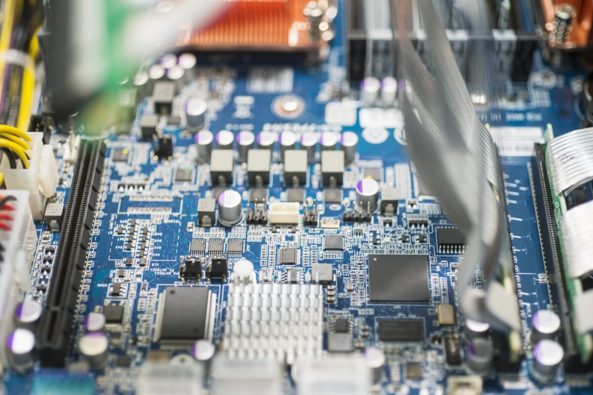
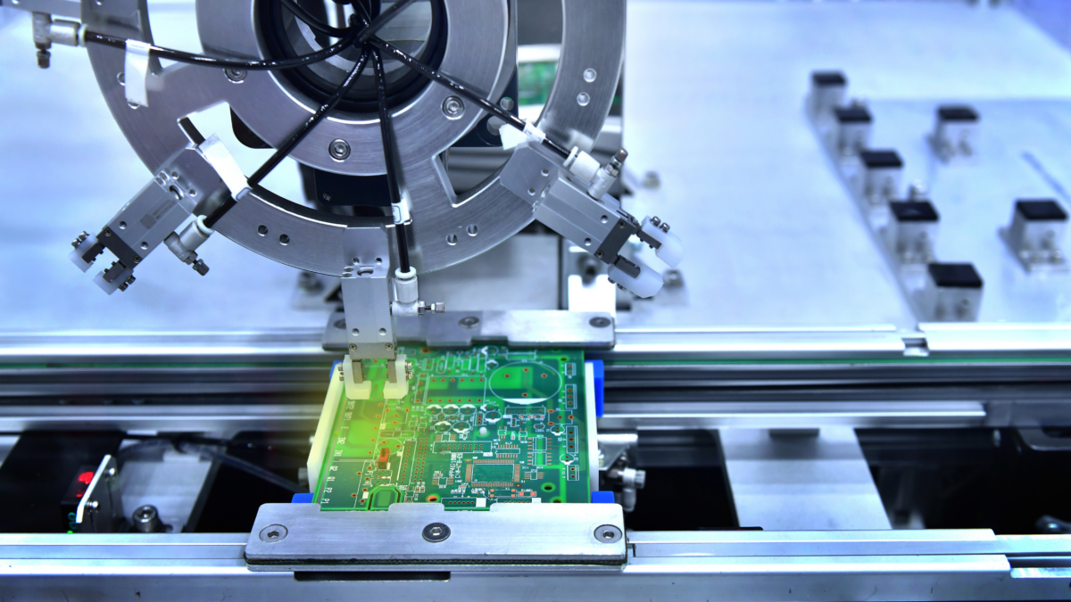
During the 1960s, double-sided circuit boards became common. One side held identification printing and the other housed electronic components. This further improved layout efficiency and performance.

Surface Mount Technology (SMT) and the Rise of Automation

One of the most important developments in the history of circuit boards came in the 1980s with the introduction of Surface Mount Technology (SMT). SMT allowed components to be mounted directly onto the surface of the board, removing the need for drilling holes as in traditional through-hole technology. This reduced assembly time, improved reliability, and enabled further miniaturization.

At Nova Engineering, our PCB assembly process includes both surface mount and through-hole technologies, depending on the specific needs of your design. Our experienced team has been at the forefront of innovation for over 35 years, and we’re proud to continue pushing the boundaries of what PCBs can do.

The Modern Era of PCB Assembly

Today, PCBs are incredibly advanced. They often include multiple layers, solder masks, silkscreens, and precision-machined traces. Materials such as fiberglass, copper, and gold plating are commonly used. Whether it’s in smartphones, medical devices, or aerospace systems, modern PCBs are the silent workhorses behind the world’s most sophisticated technology.

With the rapid growth of Internet of Things (IoT), artificial intelligence (AI), and wearable devices, the history of circuit boards is still being written. PCB design and assembly must now meet increasingly complex demands, including ultra-compact designs, high-speed data transmission, and energy efficiency.

Nova Engineering: Proud to Build the Future

At Nova Engineering, we honor the history of circuit boards by delivering exceptional service in PCB assembly, including turnkey, consigned, and partially consigned builds. With three fully equipped production lines and a dedicated prototype line, we welcome projects of all sizes and complexities.

We’ve partnered with customers for over three decades to build the technology they’re passionate about. Our strong vendor relationships and expert team ensure competitive pricing and unmatched quality.

If you’re ready to bring your next PCB project to life, contact Nova Engineering today to request a quote.

Understanding the Circuit Board Assembly Process: A Complete Guide

The circuit board assembly process is the heart of nearly every electronic device we use today—from smartphones to medical equipment. If you’ve ever wondered how these complex gadgets come to life, it all starts with a precise and highly technical process that transforms raw components into fully functional circuit boards.

In this guide, we’ll break down what the circuit board assembly process is, how it works, and why proper assembly is essential for a device’s performance and reliability.

What Is a Circuit Board?

At the core of the circuit board assembly process is the printed circuit board, or PCB. A PCB is a flat, typically green or blue board that holds and connects all the electronic components necessary for a device to function. While it may look like a simple piece of plastic, it’s actually a carefully engineered multi-layered structure composed of copper layers, insulating materials, and a protective coating.

These layers form the foundation of the circuit board assembly process, serving as both the physical platform and the electrical pathway for components like resistors, capacitors, and microchips.

The Layers Behind the Circuit Board Assembly Process

A standard circuit board used in the circuit board assembly process may have anywhere from 2 to 50+ layers, depending on the complexity of the device. These layers include:

  • Top and Bottom Layers: These are the surfaces where most components are mounted during the circuit board assembly process. They also contain antennae in certain applications.

  • Power and Ground Planes: These layers distribute power and grounding across the board.

  • Signal Layers: Internal layers route communication signals between components.

  • Insulation Layers: Fiberglass and epoxy resin insulate the copper layers and prevent electrical shorts.

  • Solder Mask and Silkscreen: The outermost coatings used to protect the copper and guide component placement.

Each part of this multi-layered system plays a critical role in the circuit board assembly process, ensuring electrical functionality and durability.

Step-by-Step: The Circuit Board Assembly Process

Now let’s walk through the key steps involved in the circuit board assembly process:

1. Solder Paste Application

The process begins with applying solder paste to the board using a stencil. This paste helps secure components to the board once heat is applied.

2. Automated Component Placement

High-speed machines then place components like ICs, resistors, and capacitors on the board with extreme precision—an essential phase of the assembly process.

3. Reflow Soldering

After placement, the board goes through a reflow oven, which melts the solder paste and creates permanent electrical connections.

4. Inspection and Quality Control

The circuit board assembly process includes both visual and automated optical inspections to detect misalignments or soldering defects.

5. Through-Hole Component Insertion (if needed)

Some designs use through-hole components, which are manually or mechanically inserted and soldered into place.

6. Final Testing

Before a board can move on to the product line, it undergoes functional and electrical testing. This stage of the assembly process ensures that every connection works as expected and that the board meets performance standards.

Why the Circuit Board Assembly Process Matters

A reliable assembly process is essential for ensuring the final product works correctly and consistently. Poor assembly can lead to:

  • Device malfunctions

  • Shortened product lifespans

  • Safety risks

  • Costly recalls and repairs

That’s why quality control, precision, and proper testing are key throughout the circuit board assembly process.

The Backbone of Modern Electronics

The circuit board assembly process is what transforms raw materials and components into the electronic brains of modern devices. Whether you’re using a smartphone, a smart thermostat, or industrial automation equipment, it’s all powered by a carefully assembled circuit board.

Understanding the assembly process helps you appreciate the complexity behind the technology we rely on every day and highlights why choosing a trusted manufacturing partner like Nova Engineering is critical to success.


Originally Published: 9/13/2021

The Future of Circuit Board Assembly: Top 5 PCB Trends of 2025

As technology advances, the future of circuit board assembly is rapidly evolving. Emerging innovations and increasing demands for efficiency, sustainability, and miniaturization are shaping how PCBs are designed and manufactured. At Nova, our team in Denver, Colorado, is dedicated to staying ahead of these changes, offering turnkey assembly, consigned assembly, and high-volume production to meet the needs of modern electronics.

What emerging technology and industry shifts will define 2025 PCB trends? Here are the Top 5 PCB Industry Trends shaping the future of circuit board assembly.

1. Miniaturization & High-Density Interconnects (HDI)

Smaller, more powerful devices drive demand for miniaturized PCB designs with high-density interconnects (HDI). As consumer electronics, medical devices, and aerospace technology shrink in size while increasing in functionality, PCB manufacturers must adopt advanced surface mount technology (SMT) and microvia techniques to fit more components in smaller spaces. Nova specializes in precision placement and compact layouts, ensuring optimal performance without sacrificing durability.

2. Automation & AI-Driven Manufacturing

Automation in PCB assembly is no longer a luxury—it’s a necessity. AI-powered automated optical inspection (AOI) and robotic soldering are transforming PCB assembly trends, enabling faster production, fewer errors, and higher efficiency. AI-driven analytics optimize workflows, reducing waste and improving quality control. At Nova, we integrate cutting-edge automation to streamline production, ensuring high-volume orders meet the highest industry standards.

3. Flexible & Wearable Electronics

The growing market for wearable tech and flexible electronics is pushing PCB manufacturers toward flexible and rigid-flex PCBs. These boards, made from polyimide or other bendable substrates, allow for curved and adaptable designs used in medical wearables, smart textiles, and automotive applications. 2025 PCB trends will see increased demand for flex-rigid PCB solutions, and Nova is well-equipped to deliver high-quality flexible circuits that meet durability and performance requirements.

4. Sustainability & Eco-Friendly Materials

As industries shift toward greener practices, sustainability is a critical factor in the future of circuit board assembly. The push for lead-free solder, recyclable PCB materials, and energy-efficient production processes is stronger than ever. Companies investing in sustainable PCB assembly will gain a competitive edge, reducing environmental impact while meeting regulatory standards. Nova is committed to eco-conscious manufacturing, sourcing high-quality, sustainable materials while optimizing processes to minimize waste.

5. Internet of Things (IoT) Integration & Advanced Connectivity

With billions of IoT devices expected by 2025, PCBs must support low-power consumption, wireless communication, and high-speed data transfer. IoT-driven applications require PCBs with multi-layer stack-ups, embedded sensors, and enhanced RF capabilities. Nova specializes in designing and assembling IoT-compatible PCBs, ensuring seamless connectivity and efficiency for smart home devices, industrial automation, and medical monitoring systems.

Looking Ahead: The Evolution of PCB Assembly

The future of circuit board assembly is defined by miniaturization, automation, flexible electronics, sustainability, and IoT-driven designs. To stay competitive, manufacturers must embrace innovation and adapt to the latest PCB assembly trends. At Nova Engineering, we leverage over 35 years of expertise, cutting-edge production lines, and a commitment to quality to help our clients bring their products to life.

Whether you need turnkey assembly, consigned assembly, or a high-volume production partner, we’re here to help. Let’s build the future of electronics—together.

Ready to take your PCB assembly to the next level? Request a quote today!

Top 5 Latest PCB Board Assembly Equipment

The process of assembling a PCB board has become both increasingly precise and technologically advanced. Whether you’re just starting to build a PCB board or you’re working with an established assembly company, the latest PCB board assembly equipment can take efficiency and accuracy to the next level. With each new breakthrough in assembly technology, the process becomes faster and more reliable, providing the foundation for cutting-edge electronics.

Here’s a rundown of the essential equipment needed for PCB board assembly in 2024:

1. Solder Paste Printing Machine

In PCB assembly, applying solder paste is the crucial first step. This paste, often a mix of tin, lead, and silver, acts as an adhesive, allowing components to securely bond to the board. The solder paste printing machine ensures a precise and consistent application of this paste onto the board’s SMD pads through the use of a stainless-steel stencil.

Today’s solder paste printers come equipped with enhanced precision capabilities, driven by AI algorithms that adapt to each board’s layout. These machines minimize waste and guarantee that solder is applied uniformly, which is vital for the success of the entire assembly process.

2. Advanced Glue Dispensing Machine

To avoid component displacement during reflow soldering, glue dots are strategically applied to the board using a glue dispensing machine. With the rapid pace of modern PCB board assembly, this machine is more critical than ever, especially for double-sided boards where components could otherwise fall off due to gravity or the force of the solder wave.

The latest glue dispensers offer adjustable speed and dispensing pressure settings, allowing manufacturers to customize glue application based on component size and layout. These features help avoid glue overflow, which can interfere with soldering and affect the functionality of the finished PCB.

3. High-Efficiency Reflow Soldering Machine

Reflow soldering remains the most widely used soldering method in PCB assembly. This process involves heating the PCB in a reflow soldering oven, where it passes through zones of increasing and decreasing temperatures. The latest reflow soldering machines feature sophisticated thermal profiling, which prevents overheating and ensures a solid bond between each component and the PCB.

Advanced models now use machine learning to monitor temperature zones and predict any potential issues before they arise. This innovation reduces the chance of defective boards and shortens the overall assembly time, which is especially valuable for large-scale PCB production.

4. Automated Optical Inspection (AOI) System

As PCB designs grow in complexity, thorough inspection becomes essential. Automated Optical Inspection (AOI) systems have become indispensable in identifying defects early in the assembly process. Modern AOI systems utilize high-resolution cameras, laser measurements, and AI-driven pattern recognition to detect issues with unmatched accuracy and speed.

The latest AOI systems in 2024 can identify even the subtlest irregularities, such as micro-cracks, tombstoning, and misalignments, which would be impossible to detect with the naked eye. These systems reduce the risk of defects reaching the final product, saving both time and material costs in the long run.

5. Functional Validation Test (FVT) Systems

Once assembly is complete, the Functional Validation Test (FVT) checks that the board performs as intended in its real-world application. Unlike earlier inspection methods, which only focused on physical flaws, FVT involves loading software onto the PCB and testing its performance within the end product environment.

The latest FVT systems offer modular testing capabilities, allowing manufacturers to quickly adapt the test parameters to different PCB designs. This flexibility is particularly beneficial as custom PCBs become more common, enabling tailored testing solutions that match the board’s end-use application.

Crafting Perfection: How Advanced Machines Revolutionize PCB Assembly

As the industry advances, manual soldering and assembly are becoming increasingly rare for large PCB production runs. With innovations in PCB board assembly equipment, companies can now build a PCB board faster and more accurately, minimizing errors and maximizing reliability. For businesses in need of high-volume, high-quality assembly, these cutting-edge machines deliver precision that meets the demands of today’s sophisticated electronics market.

What Does a PCB Do? Discover Its Role in Electronics

Printed circuit boards (PCBs) are at the heart of virtually every electronic device we rely on today. From smartphones and laptops to industrial equipment, PCBs are crucial for ensuring that electronic components function correctly and efficiently. But what does a PCB do, and why are they so important? Let’s explore the role of PCBs in modern electronics and how Nova Engineering specializes in delivering top-quality PCB solutions for various industries.

What Does a PCB Do?

A printed circuit board provides a stable platform for electronic components, such as resistors, capacitors, and integrated circuits. The PCB is responsible for connecting these components through conductive pathways, or traces, which ensure that electrical signals are properly routed. I

n essence, what do circuit boards do? They facilitate communication between the components, allowing devices to perform their intended functions. Without a PCB, it would be nearly impossible to assemble and operate complex electronic systems in an organized, efficient manner.

kinds of pcb

Kinds of PCBs and Their Uses

There are various kinds of PCB to meet different technological demands. Some of the most common types include:

  • Single-sided PCBs: These are the simplest and most cost-effective type, where components are mounted on one side, and the conductive traces are on the other.
  • Double-sided PCBs: With components and conductive paths on both sides, these are used for more complex electronics requiring additional space for circuits.
  • Multilayer PCBs: Comprising multiple layers of conductive material, these are used in advanced applications like servers, medical devices, and aerospace technologies.
  • Rigid PCBs: Rigid PCBs maintain their shape and are commonly found in computers and televisions.
  • Flexible PCBs: These can bend and are used in wearable technology, medical equipment, and consumer electronics.
  • Rigid-flex PCBs: A hybrid between rigid and flexible, these are used in highly demanding industries, such as aerospace and military applications.

Each type serves a different purpose depending on the complexity of the device, cost considerations, and required performance. Nova Engineering specializes in creating customized PCBs tailored to the specific needs of industries ranging from telecommunications to consumer electronics.

what do circuit boards do

Why Are PCBs Important?

PCBs are essential not only for their ability to organize and connect components but also for their reliability. They help protect the sensitive components from interference, excessive heat, and environmental factors that could lead to failure. Additionally, PCBs are designed to reduce the overall size and weight of devices, making them essential in the development of compact, portable electronics.

In today’s world, with the rapid advancement of technology, the need for more sophisticated and smaller electronics continues to grow. This has resulted in an increased demand for different kinds of PCBs to support innovation across industries. Whether it’s a single-sided PCB for basic electronics or a multilayer PCB for high-performance devices, the role of these circuit boards is indispensable.

Nova Engineering: Your Partner in PCB Solutions

At Nova Engineering, we understand the crucial role that PCBs play in modern technology. Our team is dedicated to designing and manufacturing high-quality PCBs that meet the exact specifications of our clients. With years of experience in the field, we provide cutting-edge solutions for industries requiring top-tier electronics performance.

Whether you’re asking, what does a PCB do for your project, or looking to explore the various kinds of PCBs for your application, Nova Engineering is here to help. Contact us today to learn more about how we can assist with your next project.

Counterfeit Components – Protecting Your PCBs from Fraud

The rise of counterfeit components is one of the most pressing threats facing today’s electronics industry. These fake parts—designed to look like genuine electronic components—are often poorly manufactured, unreliable, and incredibly difficult to detect without proper testing. For PCB manufacturers like Nova Engineering, their presence in the supply chain puts product reliability, customer safety, and brand trust at risk.

While it’s nearly impossible to eliminate every potential fraud, understanding how to reduce the risk is essential for anyone involved in printed circuit board production.

What Are Counterfeit Components?

Counterfeit components are imitation parts that are misrepresented as legitimate, branded electronic components. They may include:

  • Re-marked or relabeled parts
  • Salvaged components from discarded devices
  • Substandard replicas made with poor materials
  • Outdated or non-functioning stock sold as new

They often fail during operation, especially under stress, leading to costly product failures or, in worst-case scenarios, safety hazards—particularly in industries like aerospace, medical devices, and defense.

The Hidden Impact on Printed Circuit Boards

In many cases, counterfeit components are not discovered until after a product fails. A single bad capacitor, microcontroller, or diode can compromise an entire PCB. For companies with ongoing production or sensitive product lines, this can mean massive rework costs, production delays, or even legal liabilities.

Nova Engineering works with clients who rely on high-performance, precision-assembled PCBs. That’s why avoiding them is not just a suggestion—it’s a core part of maintaining the integrity of every build.

5 Proven Ways to Prevent Counterfeit Components in Your Supply Chain

While no method guarantees 100% protection, these five strategies significantly reduce your risk:

1. Source from Trusted Suppliers

Always purchase parts from authorized distributors or suppliers with a strong track record. Vet vendors through a detailed approval process. At Nova Engineering, we only work with component sources that adhere to strict quality assurance protocols and provide traceability documentation. If a supplier can’t confirm the origin of their parts, it’s a red flag.

2. Inspect Packaging and Labeling

Many counterfeit components are revealed through inconsistent or low-quality packaging. Watch for:

  • Misspelled words
  • Off-center logos or faded labels
  • Odd serial numbers
  • Tampered seals or repackaged parts

If something looks off, it probably is. Visual inspection should always be part of your incoming quality control.

3. Run Electrical and Functional Testing

Basic electrical tests—such as checking resistance, voltage drop, or signal output—can help identify counterfeit parts early. More advanced tests can include firmware verification or stress testing to expose failures. Nova uses robust incoming inspection methods to confirm part behavior under expected conditions.

4. Use X-ray or Scanning Inspection

Non-destructive testing like X-ray inspection can reveal internal defects, missing die structures, or inconsistent bonding—all common signs of counterfeit components. This is especially useful for ICs and high-value components where physical inspection is limited.

5. Watch for Unrealistic Pricing

If a part is being offered well below market value—especially during a shortage—it’s likely too good to be true. Opportunistic sellers often push counterfeit components when legitimate supply is constrained. Rely on market pricing data and only purchase from vetted channels.

Staying Ahead of Fraud

The global counterfeit market for electronic components continues to grow, making proactive prevention more important than ever. According to industry estimates, billions of dollars are lost annually due to faulty or fraudulent parts entering the supply chain. For manufacturers like Nova Engineering, vigilance is key.

By investing in quality control, supplier vetting, and advanced inspection techniques, we ensure every PCB we deliver is built with trusted, verified components. It’s not just about performance—it’s about protecting your end users and your reputation.

If your project demands high-reliability electronics, avoiding counterfeit components should be at the top of your priority list. At Nova Engineering, we help you stay protected from component fraud—because your product deserves nothing less.

How to Print Circuit Board with PCB Assembly Process

Our daily lives are completely dependent on electronics. Electronic components are present in everything, from our cars to our smartphones. The printed circuit board (PCB), also called the brain of these electronics, is at its core.

The majority of individuals can identify printed circuit boards when they see one. You’ll find these tiny chips covering copper and lines components at the centre of disassembled electronic gadgets. These boards are made of copper, fiberglass, and other metal components. They are joined together by epoxy and solder-masked for insulation, and this solder mask is the source of their distinctive green hue.

Let’s explore the process of printed circuit boards with the PCB Assembly Process.

Step 1: Solder Paste Stenciling

You have to apply solder paste on the board as the initial step in making PCBA. Except for using a mask, this procedure is similar to one used for shirt screen-printing. Consequently, only certain sections of the potential PCB can receive solder paste application from assemblers. The assemblers apply the solder paste where they have to place the components.

Step 2: Pick and Place

With the help of pick and place device, the PCBA process continues. Pick and place device installs mounting components or SMDs on the PCB. If you see a PCB, you will find that most non-connectors are SMDs.

Step 3: Reflow Soldering

After assembling, the assemblers ensure that the components and solder paste stays in place. Therefore, they let the solder paste dry before placing the components. Reflow is a technique used in PCB assembly to achieve this.

Once the pick and place procedure is finished, the PCB board is moved to a conveyor belt. A huge reflow oven—which resembles a commercial pizza oven—passes down this conveyor belt. The board is gradually heated to about 480 degrees Fahrenheit or 250 degrees Celsius in this oven, which is made of several heaters. This temperature will cause the solder in the solder paste to melt.

Step 4: Inspection and Quality Control

It is necessary to test the constructed board for operation once the surface mount components have been soldered during the reflow process. This does not signify that the PCBA has been completed. The movement during reflow frequently causes a connection to be of poor quality or lost entirely. This movement can occasionally result in misplaced components connecting parts of the circuit that shouldn’t be connected, leading to shorts, another frequent adverse effect.

Step 5: Through-Hole Component Insertion

Besides SMDs, there are other components on the board. But, the number of other component depends on the board’s type.The most popular type of PCB process is plated through-hole.

A PCB hole fully plated throughout is known as a plated through-hole.The holes help PCB components to transfer signals to the entire board. It is not possible to use soldering paste on this section of the board because it flows inside the hole without creating a bond between components.

Step 6: Final Inspection and Functional Test

After soldering, you have to conduct a test to check the capabilities of the board. A “functional test” is what is being performed here. This step evaluate the performance of the board while imitating the typical operating conditions. The PCB is exposed to the simulated signals and powerin this test while testers observe electrical properties.

Conclusion

The most effective method for cleaning residue off PCBs is to use a stainless-steel, high-pressure washing machine with deionized water. The gadget is not at risk while washing PCBs in deionized water, so the actual water itself—rather than the ions it contains—causes harm to a circuit. As a result, PCBs can be washed in deionized water without harm.