

Before modern advancements in electronics, connecting components in a circuit was a manual and error-prone task. Engineers relied on point-to-point wiring to create circuits inside radios, computers, and early appliances. This method was time-consuming, difficult to repair, and prone to short circuits. Everything changed when the concept of a circuit board printed with conductive paths emerged.
The shift to printed circuit boards (PCBs) revolutionized electronic design and manufacturing. Instead of hand-wiring every connection, engineers could now design a board with etched copper traces to automatically route electricity between components. This innovation drastically improved efficiency, reliability, and scalability.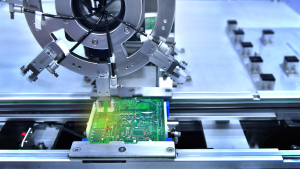
The Origins of Printed Circuit Boards
In 1936, Austrian engineer Paul Eisler introduced the first concept of a circuit board printed with copper pathways. He created a non-conductive base material with a printed copper circuit on top, which allowed components to be soldered onto predefined traces. While early versions looked nothing like today’s compact multilayer PCBs, the foundational idea remains the same.
The transition to printed technology laid the groundwork for the mass production of electronic devices. It also reduced human error and allowed for more precise circuit design, which is essential in everything from consumer electronics to aerospace systems.
How Is a Circuit Board Printed Today?
Modern PCB technology begins with a simple sheet of copper laminated onto a fiberglass-reinforced epoxy material (commonly FR4). The steps to manufacture a printed circuit board are precise and controlled to ensure quality and consistency.
1. Design and Gerber Files
The first step in creating a circuit board printed design is using computer-aided design (CAD) software. Engineers generate what’s known as Gerber files—digital blueprints that detail the layout of copper traces, pads, vias, and holes. These files drive every phase of manufacturing.
2. Drilling
Once the layout is finalized, the board undergoes a drilling process to create holes that will later hold through-hole components or vias. Each circuit board printed design includes precision-placed holes, created by computer-guided drills based on the Gerber file.
After drilling, the board is cleaned to remove any dust or debris, ensuring proper adhesion of materials in later steps.
3. Creating Copper Traces (Etching)
To create the conductive pathways, a photosensitive resist layer is applied to the copper surface. A light is used to expose only the desired circuit pattern. After exposure, the unprotected copper is removed using a chemical etching process, leaving behind the intricate network of copper traces.
This etching step is what transforms a blank copper sheet into a PCB with a custom circuit layout.
4. Solder Mask and Silkscreen
Once the traces are etched, a green (or sometimes blue, red, or black) solder mask is applied. This layer insulates the copper traces and prevents solder bridges between components during assembly.
The silkscreen layer is printed next. It provides labels, part numbers, and component identifiers directly on the circuit board printed surface, guiding technicians during assembly.
The Value of Printed Circuit Board Assemblies
A PCB with accuracy enables faster assembly, more compact device designs, and easier mass production. Whether used in smartphones or spacecraft, printed circuit boards provide the foundation for electrical functionality and performance.
Printing circuit boards also enables automation in the next stage: PCB assembly. Using automated pick-and-place machines, manufacturers can quickly place thousands of components onto a circuit board with pinpoint accuracy. Combined with reflow soldering and inspection, this results in highly reliable electronic systems.
The Role of Printing in Modern PCB Manufacturing
Today, the term printed circuit board refers not only to the physical traces on a PCB but also to the broader manufacturing process that allows for miniaturization and performance in advanced electronics. As devices become smaller and more powerful, printed circuit board technology evolves alongside them.
From its origins in early radios to powering high-speed computers, the innovation of having a circuit board printed with precise paths has transformed electronics forever. For engineers and manufacturers, it remains one of the most essential building blocks of any electronic design.
Recent Comments