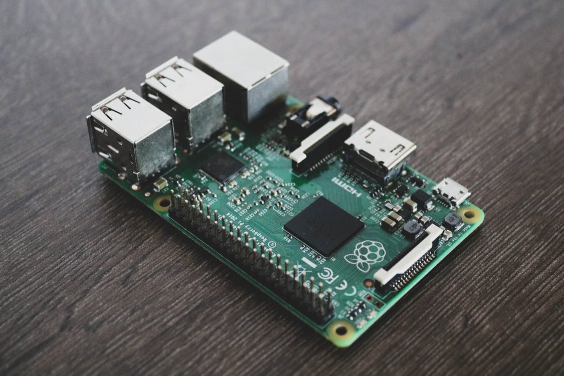
What Goes into Assembling a Circuit Board?

Do you ever wonder how and who developed the technology we use today? Well, we will not get into technical and complex details of how some things were possible, and others weren’t. This article will primarily focus on the assembly of printed circuit boards (PCB). All modern electronic and digital equipment have PCBs as an essential component.

These circuit boards are the foundation of major electrical equipment because they provide the connection for different parts and components of a digital electronic device.

Assembling a Circuit Board: Step-by-Step

If you want to assemble a circuit board on your own, you will need clear instructions and, more importantly, the right assembly guide. There are many key components that you need to consider when working on a major type of circuit board. However, when assembling a PCB, you have to be extremely careful to avoid errors, functional problems, and/or delays.

The main components of a typical PCB include a plastic or resin board that comprises different conductive and non-conductive metal parts. The silkscreen on the PCB guides the assembler on how and what connects on the board. Furthermore, you should know that the more components that a PCB requires, the longer it will take to assemble it. Let’s take a look at the four main steps of assembling your PCB below.

Step 1: Schematic Designing of the Board

You should create a schematic design before the production of the actual PCB. It serves as a silkscreen that looks like a roadmap. It means that the lines on the schematic design help to point out which component connects with what on the PCB. In general, a schematic design represents the whole circuit board. Hence, if any issues arise, they will be easy to resolve due to the schematic drawing.

Step 2: Board Design Layout

Now, the more important step. You have to convert, or more precisely, “translate” the schematic drawing into an electronic design. Bear in mind that the electronic design is present in automation software. After exporting this design in any acceptable format, you can begin the production of the board.

Step 3: Production and Assembly of the PCB

The production of the PCB is critical. You have to define all the dimensions and angles accurately to create the board finally. There are various circuit board manufacturing technologies that you can use as an assembler. The most common ones include thru-hole and surface mount technology. However, which technology you use will depend on the board’s specific requirements.

Step 4: Final Testing of the PCB

The process doesn’t end with the production of the circuit board. The last part of the assembly involves testing the board to ensure all PCB functions are achievable. The final testing phase checks and ensures that the design of the PCB is error-free and matches the schematic drawing.

Conclusion

As technology keeps evolving in various industries and fields, we have better and more efficient means of getting work done. However, technology encompasses a wide range of digital, electrical, and physical components in place. When assembling a PCB, you have to make sure that you take your time while producing schematic designs, choosing technology for production, and actually manufacturing the board. Slight errors can make the entire PCB non-functional. So, follow the step-by-step guide to ensure you don’t make any mistakes.

Reference Links:

https://www.permatechelectronics.com/the-steps-that-a-circuit-board-assembler-takes-in-pcba/blog.html

https://www.tempoautomation.com/blog/what-your-cm-wants-you-to-know-about-how-to-assemble-a-circuit-board/

https://en.wikipedia.org/wiki/Printed_circuit_board

https://www.electronicsmedia.info/2019/05/27/how-to-assemble-a-printed-circuit-board-pcb-assembly/
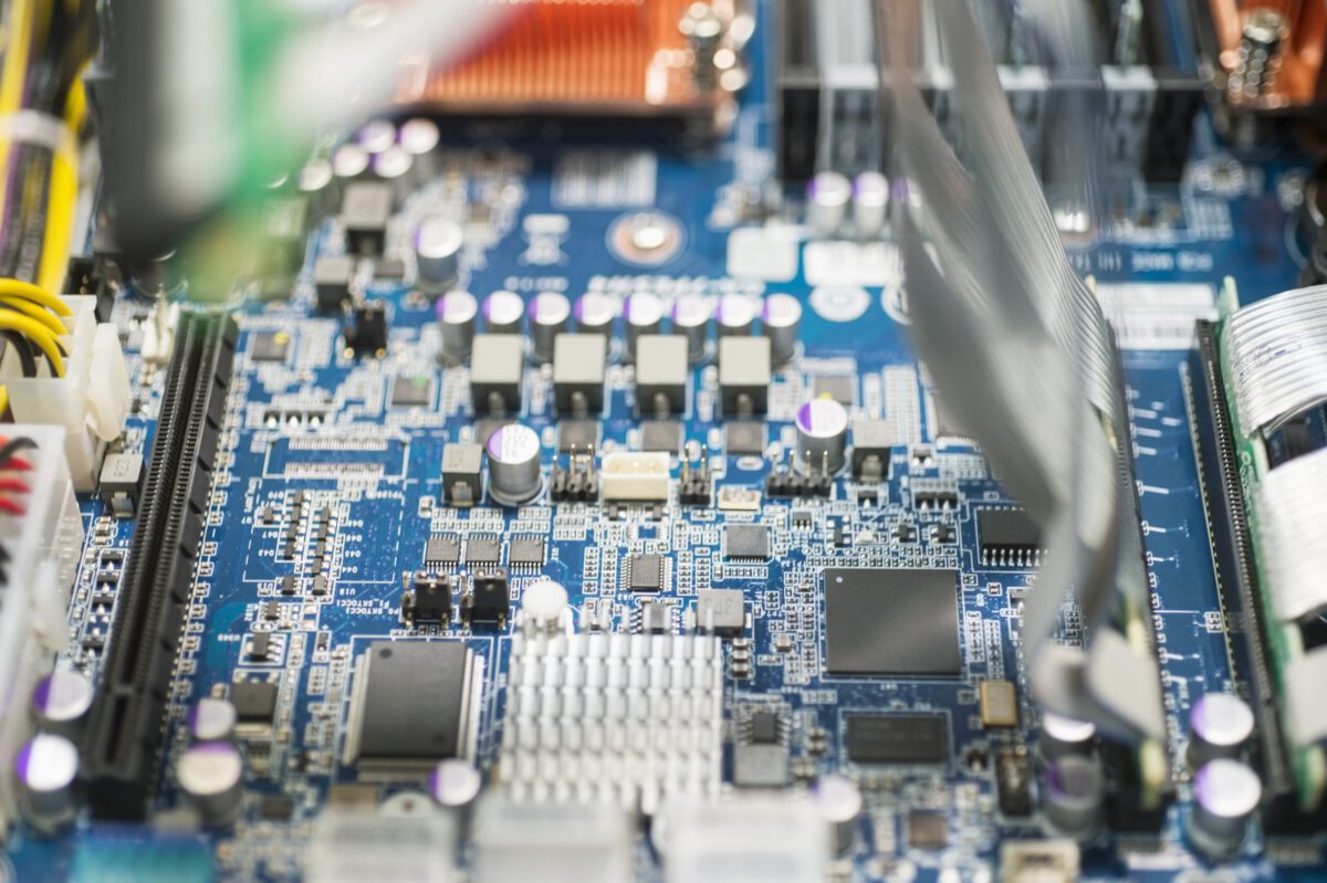
Everything You Need to Know About Circuit Board Assembly!

Most of the electrical appliances that run our lives on a daily basis include about 300 feet of tiny wires inside. This wire is the main component that adds connectivity inside an electrical product. It allows all the other small components in an electrical appliance to work seamlessly together.

The more complex an electrical appliance is, the larger the number of components and the wire inside it. However, you may be wondering where this wire is located. Well, this is where the printed circuit board assembly comes into play.

What is a PCB?

The printed circuit board or PCB is the small circuit board inside most electrical appliances. They are either green or blue and at first glance, they look like ordinary pieces of scrap plastic. But in reality, they are actually a multi-layered board that consists of an abundance of copper wires.

This scrap of flat metal is the surface on which manufacturers will precisely and carefully place all the essential components using expensive heavy machinery. Along with that, small copper wires will connect between the components and provide the necessary connectivity that occurs between all the components. This connectivity allows the components to work together and as a result, this paves the way for an electrical appliance to function.

What is inside?

The printed circuit board consists of ten conductive layers. The top and bottom layers of the Circuit board assembly make for surfaces on which manufacturers will mount components and they also act as multiple antennae. Moreover, each of these components on the circuit board requires plenty of power and ground and the PCB has entire layers that are only responsible for providing power and ground.

They are also aptly named power planes and ground planes due to their specialized role. Other ground planes that make the circuit board assembly serve the purpose of electromagnetic shielding and heat dissipation. The remaining four middle layers carry all the communication traces, which means that they carry all the signal wires.

Each of the conductive layers is copper, and between these conductive layers, there is insulating fiberglass, along with an epoxy resin that protects against the flow of electricity between the layers. A common PCB has a total of ten conductive layers, however, in a more technical and complex application, the layers can range up to 50 or more layers.

On the other hand, you may also find a PCB board that is simpler, with only two layers. Not to mention, on the top and bottom layers of a PCB, you will find a coat of solder mask, which offers a surface on which manufacturers will place components using high-tech machines. On top of the soldering mask is the silkscreen, which is nothing but the ink that indicates the placements for components by marking the circuit board.

The Assembly Process

After all the components of the PCB are manufactured, they need to be assembled before the PCB can go into the production line. This assembly process will involve the application of solder masks, automated component placement, along with the electrical testing of the bare board.

Final Thoughts

Printed circuit boards are more widely used inside computing devices, and since each model of smart phones and laptops along with other devices are different, the shapes and designs of circuit board assembly also differ vastly. Overall, it is fair to say that they are integral components of the modern technical era, and without them, none of the highest technical appliances can function.