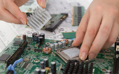
Have you ever wondered about the structure of electrons that brings your electronic devices to life? Modern electronics have the printed circuit board assembly (PCBA) process that orchestrates this structure, transforming raw components into functional devices. Every electronic device we encounter is connected to the PCB in some way. Everything from smartphones, cars, home appliances, computers, etc., has these electronic building blocks.
Deepening technological advancements and evolving with time, the PCBA process transforms a design into a fully operational circuit. Although it may seem daunting at first, it is quite easy. Before that, you must know about the components used in PCBA.
The Basic Components Of PCB
The PCBA components are essential building blocks that transform a blank circuit board into a functional electronic device. Understanding these components is crucial for anyone delving into the intricate world of Printed Circuit Board Assembly (PCBA). When carefully orchestrated, these elements breathe life into the electronic devices that have become integral parts of our daily lives. Here we tell you about the key elements:
- Integrated Circuits (ICs)
- Resistors
- Capacitors
- Inductors
- Diodes
- Transistors
- Connectors
- Resonators and Oscillators
- Microcontrollers
- Sensors
The PCBA Process Steps
Step 1. Design and Layout
The Design and Layout phase of the Printed Circuit Board Assembly (PCBA) process is the foundational stage where the blueprint of the circuit board comes to life. Designers utilize specialized software, typically CAD (Computer-Aided Design), to meticulously plan the placement of components, signal traces, and layers. This step is pivotal in ensuring optimal functionality, as a well-thought-out design directly impacts the efficiency and manufacturability of the PCB. Designers must carefully consider factors like signal integrity, thermal management, and electromagnetic interference, laying the groundwork for the subsequent stages of the PCBA process.
Step 2: Fabrication of PCB
Fabricating a PCB involves transforming the design into a tangible board. This step includes selecting appropriate substrate materials, commonly fiberglass reinforced with epoxy and copper foils for the conductive layers. The fabrication process employs techniques like etching, layering, and coating to create the final PCB. The precision and quality of fabrication significantly influence the overall performance and reliability of the electronic device.
Step 3: Component Placement
Determining how components will be placed on the PCB is critical in the PCBA process. Engineers must choose between automated assembly machines or manual labor for precise component placement. This step’s precision is crucial as it directly affects the final electronic device’s functionality and efficiency. Careful consideration is given to optimizing the use of space on the PCB.
Step 4. Soldering
Soldering is the process that brings the PCB to life by creating electrical connections between components and the board itself. There are two primary techniques: Surface Mount Technology (SMT), where components are mounted directly onto the PCB surface, and Through-Hole Technology (THT), where components are inserted into drilled holes on the PCB. Reflow soldering, a common method, involves melting solder to form secure connections. The success of the soldering step ensures the reliability of the entire PCBA.
Step 5: Inspection and Testing
After assembly, thorough inspection and testing are crucial to guarantee the quality and functionality of the PCB. Visual inspection, automated optical inspection (AOI), and X-ray testing are common quality control measures. Functional testing ensures that the assembled PCB meets performance specifications, identifying and rectifying any defects before the final product reaches the end-user.
Step 6: PCB Design Considerations
PCB Design Considerations encompass the principles and guidelines that govern the layout, trace routing, and component placement during the design phase. These considerations are essential for achieving optimal performance, signal integrity, and reliability in the final product. Factors influencing design include the type of electronic components, the intended application, and the overall goals of the electronic device.
Step 7: Fabrication of PCB
Fabricating a PCB involves transforming the design into a tangible board. This step includes selecting appropriate substrate materials, commonly fiberglass reinforced with epoxy and copper foils for the conductive layers. The fabrication process employs techniques like etching, layering, and coating to create the final PCB. The precision and quality of fabrication significantly influence the overall performance and reliability of the electronic device.
Step 8: Component Placement
Determining how components will be placed on the PCB is critical in the PCBA process. Engineers must choose between automated assembly machines or manual labor for precise component placement. The precision of this step is crucial as it directly affects the functionality and efficiency of the final electronic device. Careful consideration is given to optimizing the use of space on the PCB.
Step 9: Soldering Techniques
Soldering techniques are integral to the PCBA process, determining how components are securely connected to the PCB. Surface mount technology (SMT) involves mounting components directly onto the PCB surface, while through-hole technology (THT) involves inserting components into drilled holes on the PCB. Reflow soldering, a widely used technique, melts solder to form reliable connections, ensuring the electronic device’s durability and performance.
Step 10: Inspection and Testing
Inspection and Testing are critical steps to verify the quality and functionality of the assembled PCB. Various quality control measures are employed, including visual inspection, automated optical inspection (AOI), and X-ray testing. Functional testing ensures that the PCB meets specified performance criteria, identifying and rectifying any defects before the final product reaches the end-user.
The PCBA process is a multifaceted journey from design to a fully operational circuit. Each step plays a role in ensuring the final electronic device’s functionality, reliability, and performance. As technology advances, the PCBA process evolves, presenting new opportunities and challenges for electronic manufacturers.
Recent Comments