Everything You Need to Know About Circuit Board Assembly!

Most of the electrical appliances that run our lives on a daily basis include about 300 feet of tiny wires inside. This wire is the main component that adds connectivity inside an electrical product. It allows all the other small components in an electrical appliance to work seamlessly together.

The more complex an electrical appliance is, the larger the number of components and the wire inside it. However, you may be wondering where this wire is located. Well, this is where the printed circuit board assembly comes into play.

What is a PCB?

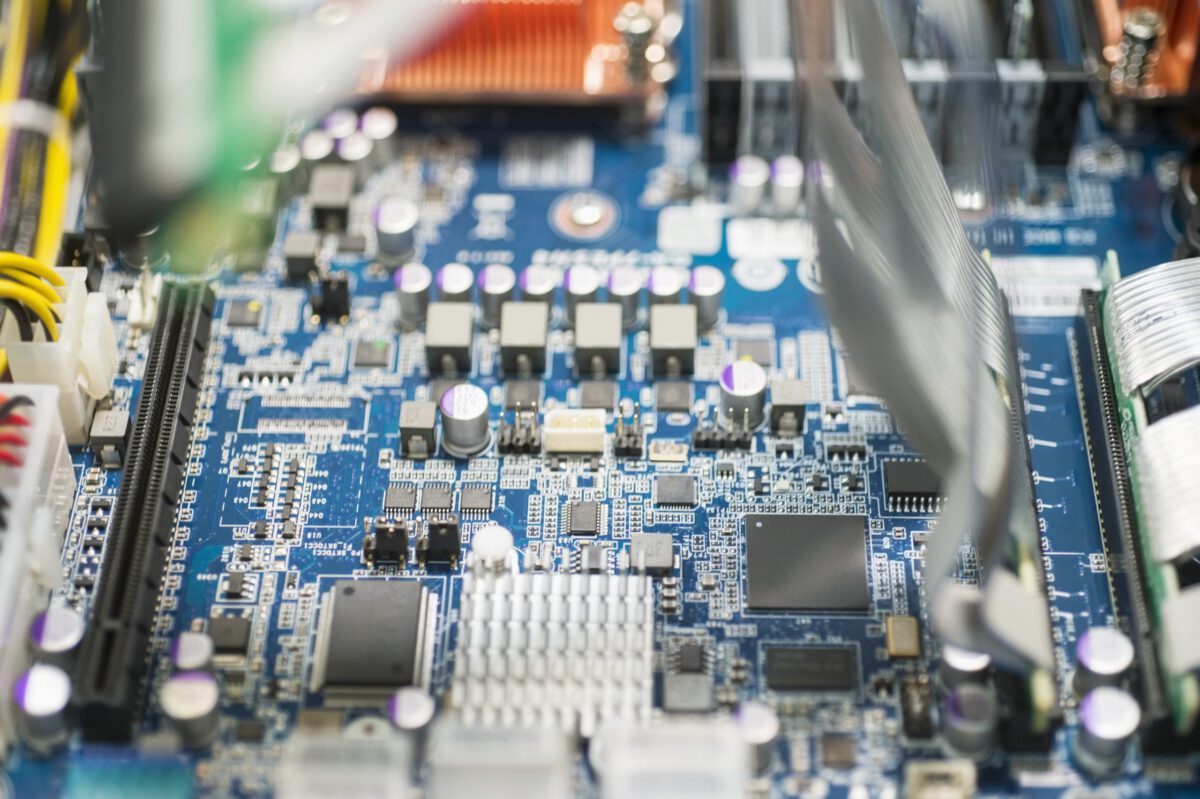
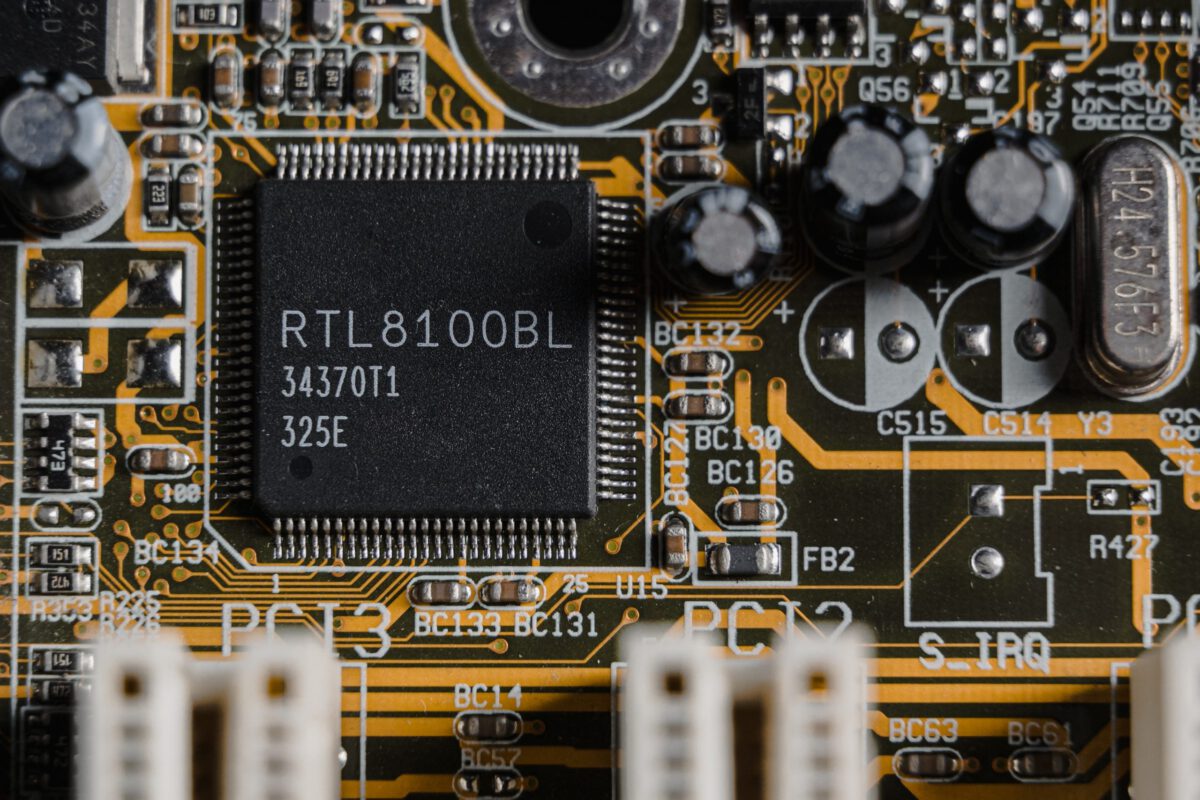
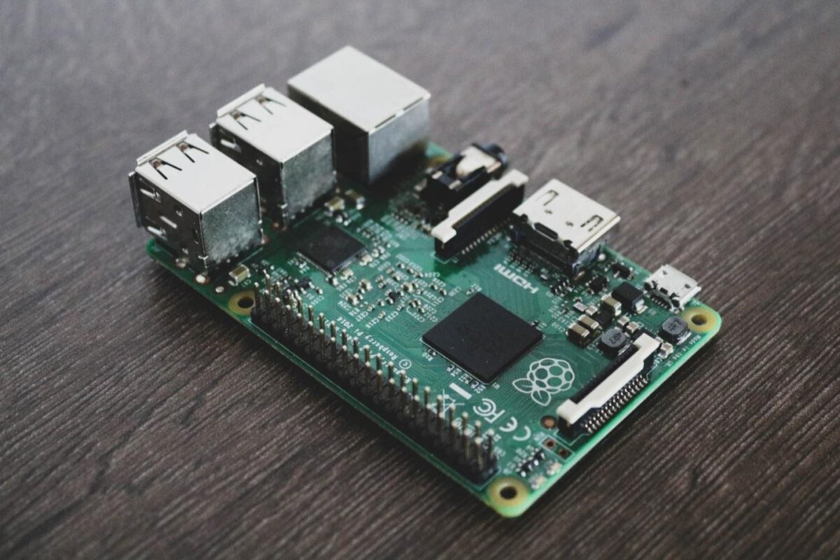
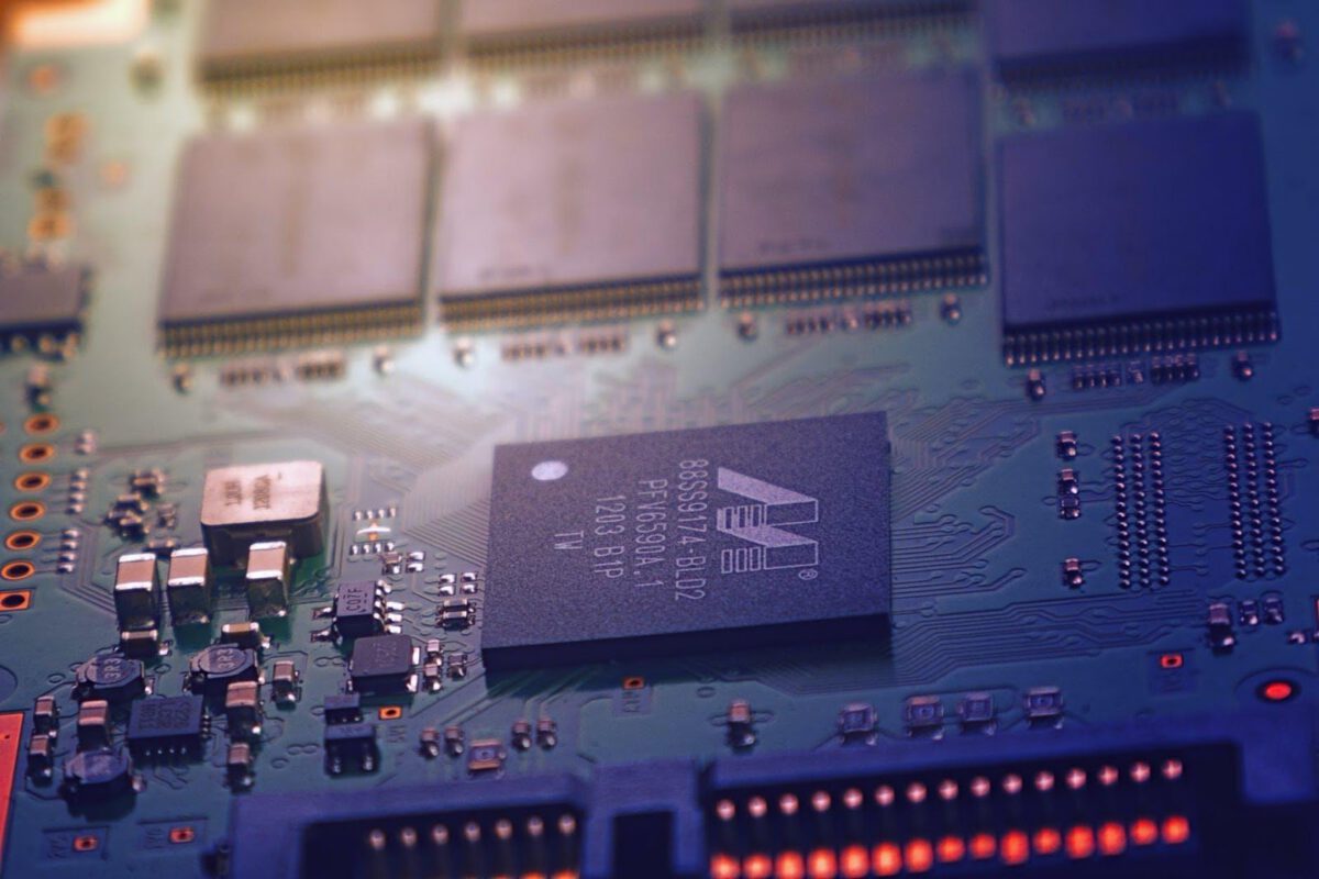
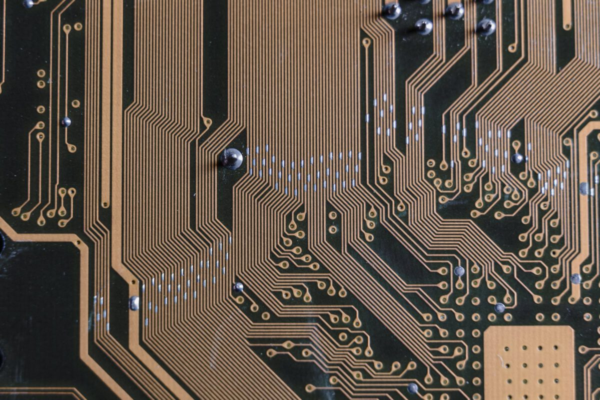
The printed circuit board or PCB is the small circuit board inside most electrical appliances. They are either green or blue and at first glance, they look like ordinary pieces of scrap plastic. But in reality, they are actually a multi-layered board that consists of an abundance of copper wires.

This scrap of flat metal is the surface on which manufacturers will precisely and carefully place all the essential components using expensive heavy machinery. Along with that, small copper wires will connect between the components and provide the necessary connectivity that occurs between all the components. This connectivity allows the components to work together and as a result, this paves the way for an electrical appliance to function.

What is inside?

The printed circuit board consists of ten conductive layers. The top and bottom layers of the Circuit board assembly make for surfaces on which manufacturers will mount components and they also act as multiple antennae. Moreover, each of these components on the circuit board requires plenty of power and ground and the PCB has entire layers that are only responsible for providing power and ground.

They are also aptly named power planes and ground planes due to their specialized role. Other ground planes that make the circuit board assembly serve the purpose of electromagnetic shielding and heat dissipation. The remaining four middle layers carry all the communication traces, which means that they carry all the signal wires.

Each of the conductive layers is copper, and between these conductive layers, there is insulating fiberglass, along with an epoxy resin that protects against the flow of electricity between the layers. A common PCB has a total of ten conductive layers, however, in a more technical and complex application, the layers can range up to 50 or more layers.

On the other hand, you may also find a PCB board that is simpler, with only two layers. Not to mention, on the top and bottom layers of a PCB, you will find a coat of solder mask, which offers a surface on which manufacturers will place components using high-tech machines. On top of the soldering mask is the silkscreen, which is nothing but the ink that indicates the placements for components by marking the circuit board.

The Assembly Process

After all the components of the PCB are manufactured, they need to be assembled before the PCB can go into the production line. This assembly process will involve the application of solder masks, automated component placement, along with the electrical testing of the bare board.

Final Thoughts

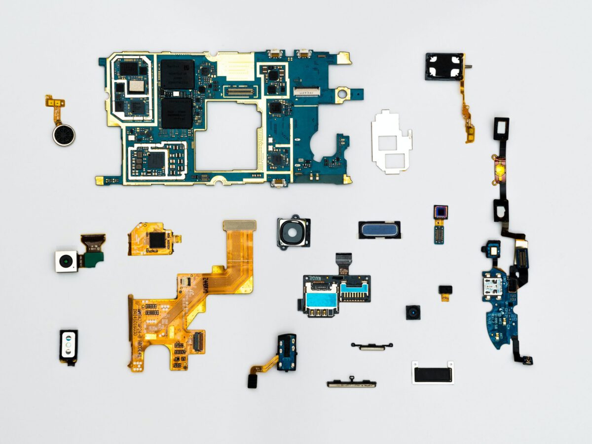
Printed circuit boards are more widely used inside computing devices, and since each model of smart phones and laptops along with other devices are different, the shapes and designs of circuit board assembly also differ vastly. Overall, it is fair to say that they are integral components of the modern technical era, and without them, none of the highest technical appliances can function.


Tips and Tricks: Learn to Improve Your Current PCB Design

Circuit designing can be incredibly daunting when it comes to practical application. Often, PCB designers will make common design mistakes that they can improve, with simple tips and tricks. In this article, you learn how to improve things such as signal integrity, EMI, and so forth.  You will also gain insights over trace widths, via sizes, placements, and clearances between traces.

Use Design Tool Kits

Often time’s people fail to realize the use-cases and benefits of tool kits, and do not utilize them for their PCB design. This is somewhat of a mistake, considering that you can find free toolkits online that can help you make a series of calculations that can help perfect a PCB circuit. It is most useful for conductor impedances, crosstalks, differential pairs, and so on.

Coupling and Decoupling Capacitors

Capacitors can come in as very handy components when building a PCB circuit. They act as timing elements or filters. When you use them as decoupling capacitor, you need to connect them in parallel with the power supply.

Why should you do this? Well, you should not expect power supply of any kind to be flawless. The output from these will have a fluctuating property. Hence, this is where a decoupling capacitor can help. Adding it into the circuit will prevent the fluctuations from the supply to reach the digital pins.

Pull Up and Pull Down Resistors

In digital circuits, the conventional way of feeding input involves using switches or push buttons. When you do that, you run into the risk of leaving the input pins into your floating state. This is where the input prints of a chip cannot detect input logic and ultimately lead to an unexpected outcome.

If you want to avoid this common floating state issue, you can use resistors of specific value to improve your PCB circuit. Resistors such as Pull up or Pull down resistors connect the input pin to VCC, so that it can read, “LOGIC 1”. Whereas, a Pull down resistor can connect the input to the ground, and you can use it to read, “Logic Zero”

Discharge Time of Batteries

Your design needs to be compatible with batteries. The most important tip, when powering your circuit with batteries, is to calculate the discharge time of the battery. This tip is helpful because if you attempt to discharge the battery capacity, more than its optimum level, you run the risk of permanently damaging your battery.

As a rule of thumb, you choice in batteries should have about 1.5 times more capacity than your circuit’s actual consumption. However, make sure to check the datasheet because of the invariabilities within the battery chemistry.

If you are designing a circuit that requires one ampere for an hour, then a battery that holds capacity of 1.5 AH is the best choice for optimum performance.

Wattage Ratings

Most people tend to forget about the wattage ratings and focus more on the resistor value of the circuit. Wattage rating of a resistor refers to the maximum amount of power that a resistor can safely dissipate in the form of heat.  If the dissipation in the resistor exceeds the maximum wattage rating, then the resistor is likely to crash.

This is why finding a wattage resistor that corresponds to your circuits resistance value is a tip that will not only improve your circuit design, but also save it from smoking. Hence, you should pay close attention to the power dissipation of a particular resistor.

To Conclude

Most of the times, it is the small changes in PCB design that make the biggest improvements. Therefore, make sure to keep track of all the small measurements and calculations if you want to optimize your circuit for it to work in its highest capacity.

How does Automated Trace Routing Work in PCB Design

Every electronic device that you use consists of over a hundred meters of wires, along with dozens of small copper components. These components work seamlessly together to run a specific electronic device, whether it is a Smartphone, television, or remote control. 

All of the wires and components perfectly attach to a thin-layered board, or PCB (Printed circuit board). When engineers mount all the components on this surface, it provides an organized framework for all the small structures to communicate with each other. 

PCB DESIGNING 

PCBs consist of conductive material that sits on insulating material, or the substrate. When you categorize PCBs based on this, you get two classifications, the single-layer PCB, and the double-layer PCB. The single-layer PCB includes a one-sided conductive coating, while the double layer has a coating on both sides. 

One of the many ways to decrease the build-up of heat in a PCB design is to widening the traces on the board. This is one of the routing rules out of many that creators follow when designing PCBs. The wider the distance between the traces, the lesser will be the resistance of the flowing current. To calculate trace widths, you can seek the help of online trace width calculators. 

Similarly, you can find methods that encompass the manual routing process. In an electronic design, automated trace routing is the way to go amidst modern technological advances.

WHAT IS AUTOMATED TRACE ROUTING?

This is a method of design for the printed circuit board, along with the integrated circuits, or (ICs). This step automates the process of placement when integrating a PCB. The dynamics of this method predicates upon identifying the placement for each active component of a PCB. 

The automated trace routing method allows you to enable an automatic routing system that systematically makes all the placements themselves. You can find auto-routing software such as Altium, which provides users an interface that helps access automated trace routing. 

With the help of automated trace routers, encoders can increase their productivity and not waste their time in manual routing solutions. 

SHOULD YOU USE AN AUTOMATED TRACE ROUTER? 

Auto-routing tools can be of immense help, especially if you are a beginner designer. They have incredible use and benefits for simpler designs. However, skilled and experienced designers that incorporate complex routing placements do not use automated routers. 

This is because the automated routing tools will often not have the complex routing strategy or layout in their systems. Therefore, whether you should use an automated trace routing tool depends entirely on the layout of your PCB, the complexity of your strategy, and the settings that you are particularly looking for.

AUTOMATED TRACE ROUTING ALGORITHMS 

Algorithms ultimately define the function of an automated trace router. They are the fundamental construct of the different routing topologies. In other words, they are a set of instructions that automate the routing process, speeding it up, and making this lengthy task easier. 

The three main algorithms for auto-routing involve random search, directed search, and river routing. Each of these algorithms has its advantages and setbacks and suits each encoder for a different set of tasks. 

TO CONCLUDE

If you are new to PCB design, then auto-routing tools can be emphatic to get you started on your PCB projects. In hindsight, the benefits of an automated trace router outweigh some of the drawbacks, especially if you consider the recent advances in their technology.

Everything You Need to Know about Solder Mask Material

Solder Mask material is a fine layer of polymer. In terms of application, engineers will often use this material for copper traces in a circuit board, PCB. It is an essential material in circuit building projects, protecting the PCB from oxidization. This is, however, not the only use case and benefit of solder masks when it comes to the construction of circuit boards.

PREVENTS THE BRIDGES FROM DEVELOPING

Printed Circuit Boards or PCB usually has components of copper placed extremely close to each other. The solder masking helps an engineer avoid solder bridges from manifesting due to the pads spaced closely.

Solder bridge refers to an electrical connection between two copper components on a PCB board. Therefore, the correct application of a Solder Mask can be instrumental in avoiding this issue. Their use case for PCBs is increasingly widespread and fine-tuned into the mass production of circuit boards.

Hence, you will not only find the solder mask material as a hand assembly use case but also integral to the mass production companies of PCB. Companies involved in mass production often use wave or reflow techniques to solder their circuits.

APPLICATION PROCESS

The application process of solder involves firstly, applying the solder material on the board, and then following it up with making openings into the material for the copper components. Engineers that craft circuit boards will make these openings, often by using photolithography techniques.

Traditionally, solder mask material has a green physical appearance, but you can find it in many other colors as well. You can also use solder-masking techniques to construct your very own solder mask at home.

Hence, the quantity, quality, or type of the solder mask material ultimately depends on the particular PCB. Every PCB is different, not only in terms of size but also in terms of applications. PCBs for certain electronic instruments may have more components than some others.
Therefore, the physical dimensions of a particular PCB, the number of openings, and the volume and sizes of components are considerations that factor in before every soldering process.

TYPES

Typically, you can find four types of solder mask materials, each having its unique physical properties and distinct applications.

TOP-BOTTOM SIDE MASKS

The use of this type of solder mask is common amongst electronic engineers. They use this type of solder to recognize the openings in the solder layer. The layering of this solder mask often follows a film or an epoxy technique.

EPOXY LIQUID SOLDER MASKS

This is one of the cheaper solder masking options since it is a polymer that you can easily silkscreen on the PCB. Silk-screening refers to a printing method in which you have to apply woven mesh to hold the ink patterns.

LIQUID SOLDER MASK/PHOTO IMAGEABLE SOLDER MASK

This solder material is often the more superior out of the four. In terms of property, it is a mixture of two different liquid components. For this reason, it has a much higher shelf life than other solder mask liquids. Furthermore, it is also versatile in its application, meaning, that you can use multiple techniques to apply this solder mask material type.

DRY FILM PHOTO IMAGEABLE SOLDER MATERIAL

This type of solder mask material is excellent for high-density wiring boards. Since the film is dry, it is less likely to escape through the holes. Moreover, when using dry film, you should use the vacuum lamination application technique.

CONCLUSION

Solder mask materials are emphatic for the PCB industry. Without their application, all circuit boards are vulnerable to damages due to short circuits. Moreover, they also have an essential role in the functionality of the particular circuit board, and they allow aspiring circuit board creators to practice their PCB crafting skills.

Flawless Prototypes and Designs Equals Perfect Circuit Board

Creating a perfect circuit board takes plenty of consideration and time. The design of the circuit board is the rudimentary and fundamental thing that contributes to the functioning of a circuit board. Creating a proper PCB design by ordering it from a proper manufacturing house is the way to go, if you wish to save time and create and flawless prototype. Below, this article will discuss how you should go about building a circuit design idea, and turning it into a prototype.  

Planning the Function of the Circuits

The first thing that you must consider before taking any circuit design measure is the function of a specific circuit. Each circuit that serves a specific circuit will have a particular design that will be distinct from other circuits with different use cases. 

Apart from the design, you also have to be varying of the components in the circuit. Each circuit that serves a specific purpose will have different components, such as resistors, batteries and controllers. Once you have a good idea of the circuit design, you can move forward and put pen to paper, and lay out a paper schematic. 

Component Sourcing and Paper Schematic 

Component sourcing involves looking at the components that you have listed down for your circuit, and finding their prices in the market. You can find your components easily online, and once you have them sorted, you can start thinking about the packages. 

The packages will describe how the circuit will physically look like. It will also determine whether you will have a THT, or an SMD.  Your package choice will lay out all the complementary components that your circuit needs.  

Next, you want to connect all the components on a piece of paper, and draw the layout of your circuit. This will also include drawing the necessary components into the right places. The package size should correspond to all the components. 

Getting a package that is too big will make your circuit look very bulky, and getting one that is too small will present you problem when attaching components. Usually, a 0.6 to 0.6 package is ideal, since it neither too big, nor too small. 

Create a Paper Schematic

You can use online schematic creators to formulate a flawless circuit system. These online paper schematic systems allow you to enter components and arrange them into orderly blocks that you find suitable. 

These online systems allow you to take what you planned on paper, and replicate it into the computer with the right dimensions. By doing so, you can implement the right techniques and get a better idea of what your circuit will look like. After doing so, you can move over to PCB design and ordering. 

PCB Design and Outline 

This is the last step of the PCB design, and involves working out the main outline of a PCB circuit. Once you have worked on the design, and ensured that the traces pair well with each other. You can go forward and order that PCB design, and get a replica that is a flawless prototype. 

To Conclude 

The introduction to online PCB design portals have made it easy and accessible for anyone to create a circuit board that is functioning and durable. However, you still need to have a good idea of design for the most efficient creation.  Let us know how we can assist you with your next project.

What Software and other Tools PCB Engineers Use?

Electronic engineers must understand the layout and design of the electrical circuits. It can be a strenuous exercise task for an engineer to work without printed circuit boards (PCBs). This is where the need for PCB designing software and tools comes into play. 

These software and tools help an engineer to design a blueprint of the PCB. Moreover, an engineer can use the software to pull old designs from the PCB libraries, customize design procedures, and verify circuits’ schematic designs. 

Basics of PCB Layout and Design Process

The success of PCB prototyping and manufacturing is a result of an immaculate design process. 

The printed circuit board design and the layout process are vital as they allow the engineer to create an error-free prototype and a flawless manufacturing process. However, the type of software and tool used to accomplish the layout and design is vital to the entire exercise. 

Before getting down to the software and tools, let us have a clear picture of the basic process of PCB design

  • Creation of schematic design
  • Capturing of schematic design
  • Determining PCB template, fixed components, card dimensions and heat sinks
  • Deciding PCB stack layers
  • Determining line impedance
  • Component placement
  • Signals trace routing
  • Generating Gerber file

Software and Tools Engineers Use

Engineers use several software and tools to complete the above-mentioned process efficiently and precisely. 

Electronic Design Automation (ECAD) Tool

This one is a category of design tools used for the process of schematic design capture. These tools work simultaneously in the modular design flow to produce PCB’s design description. Some of the most popular tools that fall within the ECAD category are as follows. 

  • ORCAD

The PCB design engineers use this software to create an electronic schematic and blueprint of the circuit board. 

  • EAGLE

EAGLE is an acronym for “Easily Applicable Graphical Layout Editor.” This software is a solution-driven design program for printed circuit boards. EAGLE contains a PCB layout editor, schematic capture editor, Bill of Material Tools (BOM), and auto-router. 

  • PADS

PADS is a layout tool that contains advanced analysis, schematic designs, and, most notably, the feature to collaborate from ECAD to MCAD. 

5 Popular Designing Software and Tools Used by PCB Engineers

Although there is a wide range of PCB designing software and tools available in the market, here are the top five. 

  1. Altium Designer – it is famous for its feature to simulate your printed circuit board using the Altium PCB software. 
  2. PCB Artist – this software by Advanced Circuits is famous for its best shipping record and active consumer base. If you are looking for an intuitive solution for PCB designing, look no further. 
  3. SolidWorks PCB – this one has a robust design technology with ease-of-use. You will also get an on-demand bidirectional mixing feature along with the flawless collaboration of CAD and PCB designs. 
  4. Ultiboard – this PCB designing software by National Instruments allows you to leverage modular hardware and an expansive ecosystem. You can benefit from a quick prototyping atmosphere and save hours on the development phase. 
  5. DipTrace – if you are looking for a comprehensive design solution, smart manual routing, and shape-based auto-route, DipTrace is the answer. This software has a single environment that enables you to benefit from the direct conversion circuit to board feature and revise the schematic annotations in run-time. 

Tips and Considerations: Learn to Improve Your PCB Design Skills

Are you a printed circuit board (PCB) engineer wondering how you can learn or improve your PCB design skill? Well, you are in the right place, as this post will give you a brief insight into tips and considerations that can help you polish your skills. 

Most engineers are good at PCB designs. However, they lack some basic professional and personal skills they must master. You must begin with the basics and learn to practice your PCB designing skills with consistency day-in and day-out. 

5 Tips to Improve Your PCB Design Skills

Here are five basic tips to improve your printed circuit board designing skills.

  1. Learning more about the Layers

In case you wish to master the skills of designing a multi-layered PCB, you must have a clear understanding of printed circuit board layers. You must learn to revise your basics and learn about the latest standards and trends to ensure that your PCB design meets all the industry and global standards. 

  1. Remembering the Design Rules

There are numerous design rules that every PCB design engineer must follow. Some of the most essential ones are as follows. 

  • Aim for noise reduction
  • Remember the EMI/EMC considerations
  • Remember the thermal integrity considerations, i.e., dissipation of heat because of the power circuits. 
  • Remember the power integrity considerations, i.e., power loss in its path
  • Learn to design for test and add test points at several stages of design. 
  • Follow the design for manufacturing ideology. Always consider track width, drill size, clearance, etc. 
  1. Learning to Use PCB Designing Software 

As designing technology has evolved, using PCB design software is common. In case you are not good at using software, you must polish your skills to draw components, schematics, and printed circuit board layouts. 

There are several PCB designing software solutions available in the market. However, you must pick a few that are common in your industry. If you are enthusiastic about learning more than one design software, then this will give you a competitive edge over other designers and engineers when searching for a new job. 

  1. 3-D Modeling

While you learn to design a printed circuit board on software, do not forget to add a 3-D modeling feature into it. This will allow you to see an almost real depiction of your PCB design before manufacturing it. 

Moreover, this will also allow you to detect any design errors and help save back-and-forth revisions with the PCB assemblers. This will translate into lower cost and time efficiency. 

  1. Learning to Review Thoroughly

So, you have learned the standards. You know the layers and know how to use software to create a 3D model of your printed circuit board. What is next? 

You must always learn to improve your attention to detail. This is very critical if you wish to get your PCB design right the first time. This will again save you from a lot of hassle in the future because the tiniest flaw in the design may result in several revisions and sometimes the overhauling of the entire printed circuit board design. 

Here, you can also learn about the basics of documentation and aesthetics. This will allow you not only to write how the components’ placement should be but also customize how the PCB design must feel and look. 

The documentation part will allow you to clearly label where each component and connector must go and how it must look on the printed circuit board

 The Take-Away

Learning all of the above skills will allow you to improve your PCB design skills as well as learn how to document the guidelines for the assemblers. The more elaborate you are in your design, the better the results.  At Nova, we are always updating and improving our skills. Reach out for a consultation today.

There’s more than one Reason to Make a Flawless Printed Circuit Board

A printed circuit board (PCB) is a very critical part of our modern-day electronic equipment. Your basic printed circuit board usually consists of large active and passive components. These components have side-to-side connections with each other that you can see via traces on the board. 

You can actually create larger circuits using smaller printed circuit boards using small-sized components. However, you must ensure to make a flawless PCB to make them a perfect choice for any manufacturer of electronic components, equipment, and instruments. 

Let us dive right in and see how making a flawless printed circuit board can help. 

7 Reason to Create Flawless Printed Circuit Boards

Here are seven of the fundamental but essential reasons why you must create flawless PCBs. 

  1. Saves Time and Energy

While traditional circuit board connection methods can take longer to connect each component, the PCB takes less time to assemble a circuit. 

  1. Compact Size 

If you are designing a characteristically printed circuit board, it will include numerous electronic components.  Instead of using current-carrying wires, you use copper tracks to interconnecting the components on a PCB. This gives your PCB finesse, compact design, and lightweight. 

A perfect PCB design will offer you a simple platform to arrange sophisticated electronic components in an efficient manner. This compactness enables you to create complicated and bigger electronic circuits in smaller form factors. 

  1. Preventing Lose Connections and Short Circuits

Creating a flawlessly printed circuit board will allow you to use copper tracks. This means there will be no chances of any short circuits or loose connections. 

  1. Ease To Repair

In case your PCB incurs damage, you can easily run a diagnostic on it to check and replace the failed components. The properly designed printed circuit board has clear labels for each electronic component mentioning their polarities. 

This also allows you the convenience to install and/or repair the board and its components. 

  1. Reduced Electronic Noise

A printed circuit board produces less electronics noise. The reason is that the organization of the component is so precise that the electrical current’s path between them is as smaller as possible. This translates into low radiation as well as reduced pick up of any electromagnetic waves. 

This also ensures minimal crosstalk between any of the electronic components and their varied traces. This is actually a big concern in traditional circuit boards. The electronic noise usually releases in the form of radiation, heat, and flickering sounds. 

  1. Cost-Effectiveness and Reliability 

Printed Circuit Boards are very cheap to manufacture, especially during mass production. Moreover, they offer reliability to the performance of your circuits. 

  1. Fixed Components

One of the most important advantages of designing a flawless printed circuit board is that all the components are firmly fixed to the board. The manufacturers use solder flux, which ensures that the components do not move from their place irrespective of how much you move the board.

Conclusion

Manufacturing a printed circuit board will cost you money. Therefore, you must ensure that you design a flawless specimen instead of getting issues from the assemblers or clients. It would be wise to involve your printed circuit board assemblers’ team from the beginning. 

This will allow you to gain valuable insight into how you can start making an impeccable printed circuit board design. Moreover, the assemblers can also give you valuable information about the new practices, trends, and materials to make flawlessly printed circuit boards. The more knowledge you have, the better your printed circuit board will be. In case you are looking for international standards. You can check out the Institute of Printed Circuits (IPC), as they are the global entity setting standards for printed circuit board designing, manufacturing, and assembly. We are also available to consult with you on any of your PCB needs.