What Goes into Assembling a Circuit Board?

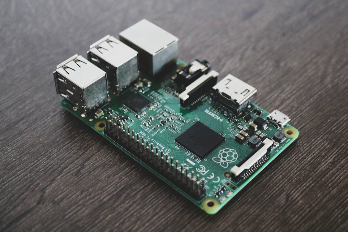
Do you ever wonder how and who developed the technology we use today? Well, we will not get into technical and complex details of how some things were possible, and others weren’t. This article will primarily focus on the assembly of printed circuit boards (PCB). All modern electronic and digital equipment have PCBs as an essential component.

These circuit boards are the foundation of major electrical equipment because they provide the connection for different parts and components of a digital electronic device.

Assembling a Circuit Board: Step-by-Step

If you want to assemble a circuit board on your own, you will need clear instructions and, more importantly, the right assembly guide. There are many key components that you need to consider when working on a major type of circuit board. However, when assembling a PCB, you have to be extremely careful to avoid errors, functional problems, and/or delays.

The main components of a typical PCB include a plastic or resin board that comprises different conductive and non-conductive metal parts. The silkscreen on the PCB guides the assembler on how and what connects on the board. Furthermore, you should know that the more components that a PCB requires, the longer it will take to assemble it. Let’s take a look at the four main steps of assembling your PCB below.

Step 1: Schematic Designing of the Board

You should create a schematic design before the production of the actual PCB. It serves as a silkscreen that looks like a roadmap. It means that the lines on the schematic design help to point out which component connects with what on the PCB. In general, a schematic design represents the whole circuit board. Hence, if any issues arise, they will be easy to resolve due to the schematic drawing.

Step 2: Board Design Layout

Now, the more important step. You have to convert, or more precisely, “translate” the schematic drawing into an electronic design. Bear in mind that the electronic design is present in automation software. After exporting this design in any acceptable format, you can begin the production of the board.

Step 3: Production and Assembly of the PCB

The production of the PCB is critical. You have to define all the dimensions and angles accurately to create the board finally. There are various circuit board manufacturing technologies that you can use as an assembler. The most common ones include thru-hole and surface mount technology. However, which technology you use will depend on the board’s specific requirements.

Step 4: Final Testing of the PCB

The process doesn’t end with the production of the circuit board. The last part of the assembly involves testing the board to ensure all PCB functions are achievable. The final testing phase checks and ensures that the design of the PCB is error-free and matches the schematic drawing.

Conclusion

As technology keeps evolving in various industries and fields, we have better and more efficient means of getting work done. However, technology encompasses a wide range of digital, electrical, and physical components in place. When assembling a PCB, you have to make sure that you take your time while producing schematic designs, choosing technology for production, and actually manufacturing the board. Slight errors can make the entire PCB non-functional. So, follow the step-by-step guide to ensure you don’t make any mistakes.

Reference Links:

https://www.permatechelectronics.com/the-steps-that-a-circuit-board-assembler-takes-in-pcba/blog.html

https://www.tempoautomation.com/blog/what-your-cm-wants-you-to-know-about-how-to-assemble-a-circuit-board/

https://en.wikipedia.org/wiki/Printed_circuit_board

https://www.electronicsmedia.info/2019/05/27/how-to-assemble-a-printed-circuit-board-pcb-assembly/
Everything You Need to Know About Circuit Board Assembly!

Most of the electrical appliances that run our lives on a daily basis include about 300 feet of tiny wires inside. This wire is the main component that adds connectivity inside an electrical product. It allows all the other small components in an electrical appliance to work seamlessly together.

The more complex an electrical appliance is, the larger the number of components and the wire inside it. However, you may be wondering where this wire is located. Well, this is where the printed circuit board assembly comes into play.

What is a PCB?

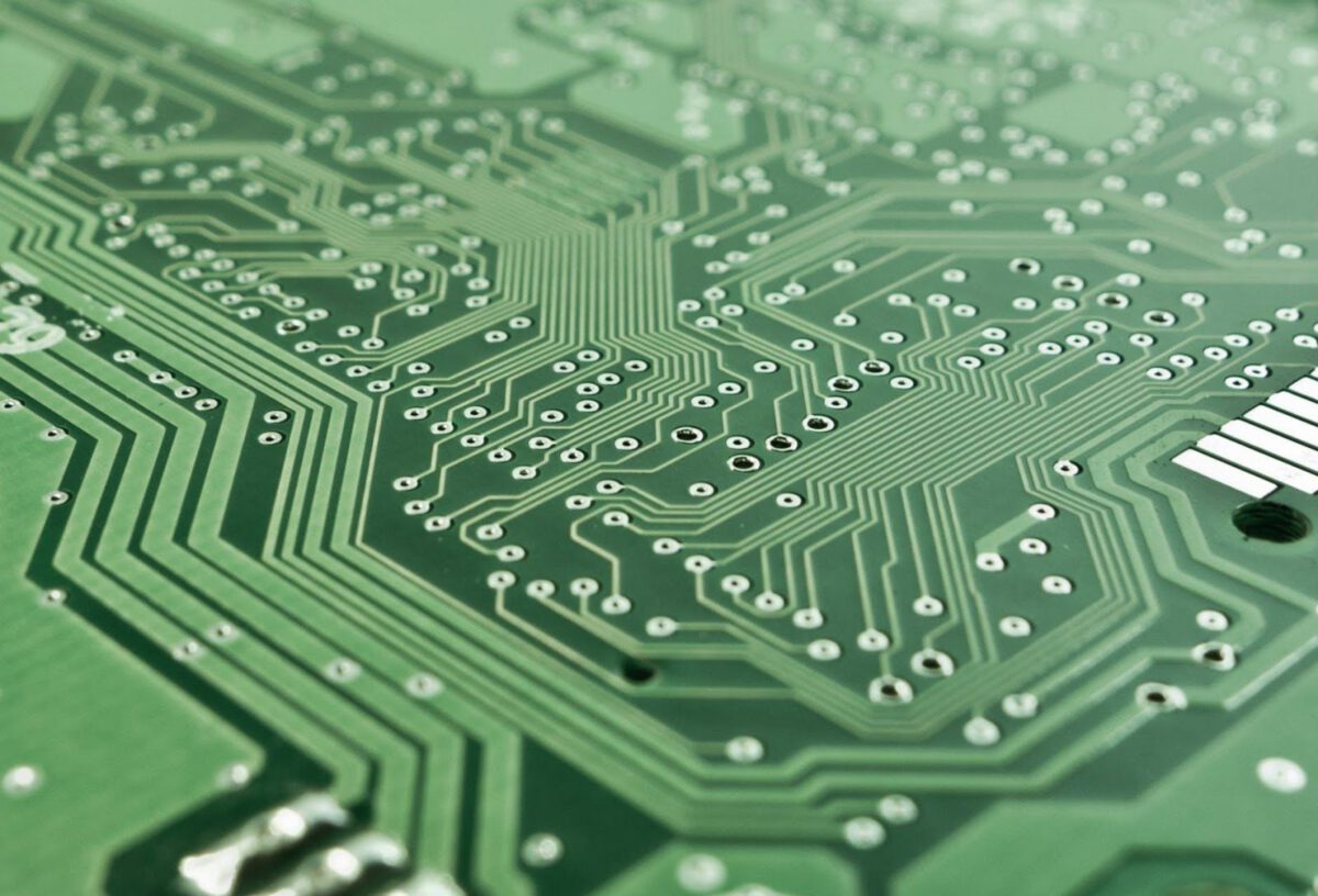
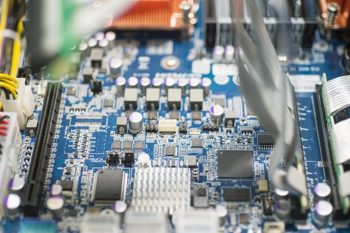
The printed circuit board or PCB is the small circuit board inside most electrical appliances. They are either green or blue and at first glance, they look like ordinary pieces of scrap plastic. But in reality, they are actually a multi-layered board that consists of an abundance of copper wires.

This scrap of flat metal is the surface on which manufacturers will precisely and carefully place all the essential components using expensive heavy machinery. Along with that, small copper wires will connect between the components and provide the necessary connectivity that occurs between all the components. This connectivity allows the components to work together and as a result, this paves the way for an electrical appliance to function.

What is inside?

The printed circuit board consists of ten conductive layers. The top and bottom layers of the Circuit board assembly make for surfaces on which manufacturers will mount components and they also act as multiple antennae. Moreover, each of these components on the circuit board requires plenty of power and ground and the PCB has entire layers that are only responsible for providing power and ground.

They are also aptly named power planes and ground planes due to their specialized role. Other ground planes that make the circuit board assembly serve the purpose of electromagnetic shielding and heat dissipation. The remaining four middle layers carry all the communication traces, which means that they carry all the signal wires.

Each of the conductive layers is copper, and between these conductive layers, there is insulating fiberglass, along with an epoxy resin that protects against the flow of electricity between the layers. A common PCB has a total of ten conductive layers, however, in a more technical and complex application, the layers can range up to 50 or more layers.

On the other hand, you may also find a PCB board that is simpler, with only two layers. Not to mention, on the top and bottom layers of a PCB, you will find a coat of solder mask, which offers a surface on which manufacturers will place components using high-tech machines. On top of the soldering mask is the silkscreen, which is nothing but the ink that indicates the placements for components by marking the circuit board.

The Assembly Process

After all the components of the PCB are manufactured, they need to be assembled before the PCB can go into the production line. This assembly process will involve the application of solder masks, automated component placement, along with the electrical testing of the bare board.

Final Thoughts

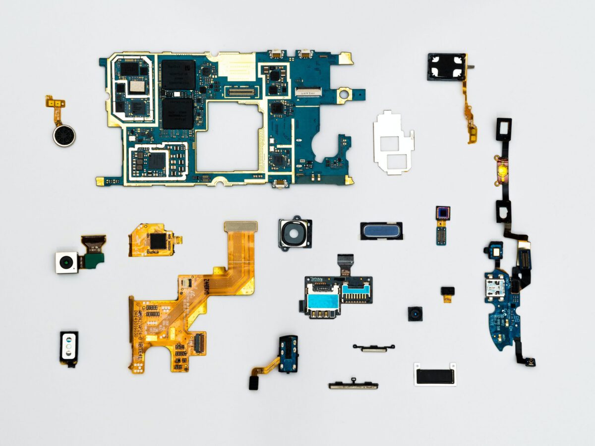
Printed circuit boards are more widely used inside computing devices, and since each model of smart phones and laptops along with other devices are different, the shapes and designs of circuit board assembly also differ vastly. Overall, it is fair to say that they are integral components of the modern technical era, and without them, none of the highest technical appliances can function.


The Process of a Printed Circuit Board Assembly

The PCB assembly process undergoes thorough and intricate steps. PCB’s being the staple circuit board mechanism in most of the electronic appliances is undoubtedly major components that require perfect assembly otherwise they can be major causes of concern for many industries.

BluePrints and Layouts

The assembly process in factories start with a framework or blue print layout and make their way to the customers. Due to the advancements in PCB production, modern manufacturing units hardly have any workers on the production floor. This is because most of the manufacturing process is subject to automation and efficient machinery.

In the starting stage of assembly, the burr board inserts into the laser marking machine, which marks a serial number on the board so that the board can have a manufacturing label. This process is common in large scale production, but is not something common to all Printed circuit board manufacturers.

Applying Solder Mask

The process initiates with the application of solder to the circuit board. Solder mask is a material that sits on top the circuit as a layer in which you can install components of the circuit board. A specific inspection machine then inspects the circuit board and ensures that it is aligned.

Once the inspection is complete, it applies solder all the way across the surface board in an evenly fashion. After solder application, the solder goes through another inspection to ensure that it is applied evenly.  Once the inspection is complete, the board is ready to undergo the next stage.

Adding Component Placements

The next stage involves the addition of the placements. Machines rapidly add placements on the board that are coming from the reels. This machine includes heads that pick up the reels and attaches them to the circuit board. This reel placement happens for about eight times before the circuit board is ready for the next stage.

After all the components attach to the board, it is then ready for the reflow process. This process is important since the solder needs to melt so that it can adhere and be a good surface that provides mechanical and electrical connections between components and parts.

Reflow process

When it goes under the cooking process of the machine, it comes out from the other side to cool. Cooling process takes place so that all the junctions between the components can form and solidify. This results in the next step which involves testing.

Inspection and Electrical Testing

The final inspection will now ensure that all the components are situated in their correct specific placements so that the circuit board assembly is ready for use.  In this testing, advanced machines identify whether the pins are contacting the pads in the exact location. At this point, the SMT process is in completion.

Electrical testing can have implications that follow two processes. The first involves the bed of nails, which helps manufacturers test at a high volume at a shorter time, however it require expensive fixtures. The second testing method is a flying probe, which is a high mix at a small volume.

If the circuit board assembly includes large BGA components, then manufacturers need to inspect whether the pins are reaching the right layer.  These pins are usually behind each component and therefore, you cannot test those using automated machines. In this scenario, manufacturers will likely use the help of X-ray images and make sure that the soldering and components are adequate.

Parts of a PCB, or Printed Circuit Board

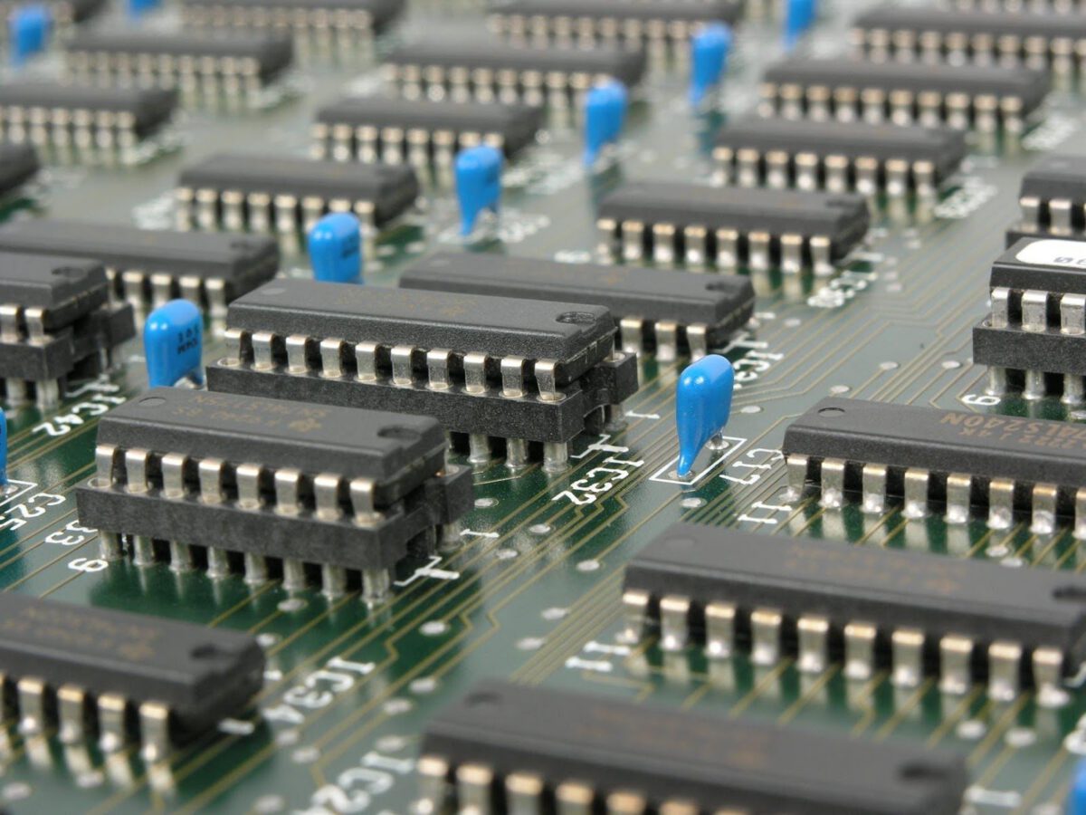
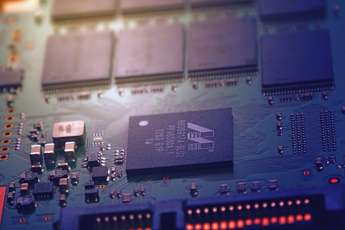
Whether the PCB board is inside an air conditioner, or a refrigerator, you can find numerous different parts mounted on the bare board. The main components that you are likely to find and which are critical for its functioning involve a Fuse, transformer, and a switch. The quantity and types of these components can vary according to the specific electrical appliance.

To Conclude

All of these processes and testing are then finalized by a functional test. As you can see, the process of a printed circuit board assembly is full of inspections and automated machine work. Thus, it is a true reflection of the detailed workings in a mass production factory.


Tips and Tricks: Learn to Improve Your Current PCB Design

Circuit designing can be incredibly daunting when it comes to practical application. Often, PCB designers will make common design mistakes that they can improve, with simple tips and tricks. In this article, you learn how to improve things such as signal integrity, EMI, and so forth.  You will also gain insights over trace widths, via sizes, placements, and clearances between traces.

Use Design Tool Kits

Often time’s people fail to realize the use-cases and benefits of tool kits, and do not utilize them for their PCB design. This is somewhat of a mistake, considering that you can find free toolkits online that can help you make a series of calculations that can help perfect a PCB circuit. It is most useful for conductor impedances, crosstalks, differential pairs, and so on.

Coupling and Decoupling Capacitors

Capacitors can come in as very handy components when building a PCB circuit. They act as timing elements or filters. When you use them as decoupling capacitor, you need to connect them in parallel with the power supply.

Why should you do this? Well, you should not expect power supply of any kind to be flawless. The output from these will have a fluctuating property. Hence, this is where a decoupling capacitor can help. Adding it into the circuit will prevent the fluctuations from the supply to reach the digital pins.

Pull Up and Pull Down Resistors

In digital circuits, the conventional way of feeding input involves using switches or push buttons. When you do that, you run into the risk of leaving the input pins into your floating state. This is where the input prints of a chip cannot detect input logic and ultimately lead to an unexpected outcome.

If you want to avoid this common floating state issue, you can use resistors of specific value to improve your PCB circuit. Resistors such as Pull up or Pull down resistors connect the input pin to VCC, so that it can read, “LOGIC 1”. Whereas, a Pull down resistor can connect the input to the ground, and you can use it to read, “Logic Zero”

Discharge Time of Batteries

Your design needs to be compatible with batteries. The most important tip, when powering your circuit with batteries, is to calculate the discharge time of the battery. This tip is helpful because if you attempt to discharge the battery capacity, more than its optimum level, you run the risk of permanently damaging your battery.

As a rule of thumb, you choice in batteries should have about 1.5 times more capacity than your circuit’s actual consumption. However, make sure to check the datasheet because of the invariabilities within the battery chemistry.

If you are designing a circuit that requires one ampere for an hour, then a battery that holds capacity of 1.5 AH is the best choice for optimum performance.

Wattage Ratings

Most people tend to forget about the wattage ratings and focus more on the resistor value of the circuit. Wattage rating of a resistor refers to the maximum amount of power that a resistor can safely dissipate in the form of heat.  If the dissipation in the resistor exceeds the maximum wattage rating, then the resistor is likely to crash.

This is why finding a wattage resistor that corresponds to your circuits resistance value is a tip that will not only improve your circuit design, but also save it from smoking. Hence, you should pay close attention to the power dissipation of a particular resistor.

To Conclude

Most of the times, it is the small changes in PCB design that make the biggest improvements. Therefore, make sure to keep track of all the small measurements and calculations if you want to optimize your circuit for it to work in its highest capacity.

PCB Finishes: Immersion Silver

It is a well-known fact that printed circuit boards (PCBs) use copper surface finishes as a common practice. If left unattended and unprotected, copper will deteriorate and oxidize, leaving your circuit board unusable. 

A surface finish plays a vital role in creating an interface between a PCB and its components. Here are two of the main functions of a surface finish.

  • It helps protect the copper-based circuitry
  • It provides you surface that can facilitate soldering during the assembling process of soldering components to your PCB

What Is Immersion Silver?

Immersion silver surface finish is a type that you can apply directly over your printed circuit boards’ copper surface. This surface finish is most commonly used and ideal for metallic dome contacts, aluminum wire bonding, and EMI shielding. 

The thickness of this material is between 5 micro-inches and 12 micro-inches, respectively. Additionally, immersion silver has lasting capabilities for at least a year. 

Immersion silver surface finish does not react to copper the way Tin does. However, if you expose it to the air, it will tarnish; therefore, you must store the circuit boards with immersion silver finish in an anti-tarnishing packaging. 

If you do everything right and store it in proper packaging, the PCB will still be solderable for 6 to 12 months. However, once you have removed your printed circuit board from the packaging, you must make sure that it goes through soldering re-flow within the next 24 hours.

In case you wish to achieve a higher shelf life than gold, plating is the most viable solution. 

Benefits of Immersion Silver Surface Finish

PCBs always come with coated surface finishes. Adding a decent finish enables and ensures decent soldering capability, as well as it protects the copper circuitry of your circuit board from the outside air. There are several types of immersion finishes, such immersion tin, immersion gold, etc.; however, immersion silver is gaining popularity due to certain features it offers. 

It is attracting a lot of attention from the PCB manufacturers. Here are some of the key advantages that declare it to be the preferred material for surface finishing in the circuit board industry. 

  • It allows the proper spreading of solder on its surface, allowing better soldering of circuit board components. 
  • Immersion is one of the RoHS compliant PCB surface finishes, and it is also environmentally friendly. 
  • Compared to OSP “Organic Solderability Preservative” surface finish, the surface with immersion silver finish will demonstrate better resistance to several environmental aging factors. 
  • The immersion silver is a material surface finish that comes with the capabilities to survive multiple re-flows. 
  • Immersion silver has better and enhanced electrical properties. 
  • It produces a flat surface and facilitates strengthened solder joints than HASL surface finish. 
  • Immersion silver is immune to a phenomenon known as a black-pad interfacial fracture. 

All of the advantages mentioned above make immersion silver surface finish an ideal choice for PCB manufacturers. 

Choose Wisely

You must select an adequate surface finish for your PCBs. You can do so by considering several options while you factor material costs and performance requirements. 

For instance, you are looking for an option that is lower in cost than Tin-Lead. HASL may sound like a more obvious choice, but it is not the most suitable option, especially when it comes to RoHS compliant products. 

In case you are unsure of what type of surface finish you may need. You can always get help from third-party PCB fabrication services prior to making decisions you may regret later. A little bit of research will result in cost-effective and high-yielding design.  We are here to answer any questions you may have and help you make the best decision for you. Contact us today!

Cost Reduction Ideas for Your Next PCB Assembly Project

Are you looking for ways to reduce the overall cost of your next PCB assembly project? If your answer is a ‘yes,’ you are in the right place. 

A fundamental way to contribute to your organization financially is by adopting cost-effective methods to reduce the total cost of printed circuit board assembly projects. You can take many steps to reduce the cost of a PCB assembly project. 

3 Smart Cost Reduction Tips for PCB Assembly Project

Although you can surely make some internal changes in the assembly process and find the vendors offering competitive rates, here are the three most essential tips above all.

Tip # 1 – Providing Multiple Sources for Each Component of the Circuit Board

You must always avoid a single source to procure your components as much as possible. Why? There are several advantages to having multiple procurement sources. 

For instance, you can ensure greater availability of components required for distribution with multiple component procurement sources. Moreover, you can also have the leverage to bargain for components’ costs due to competition in the market. 

The biggest problem associated with single sourcing is, you can end up with a shortage of parts. This may hinder your manufacturing process. Thus, you can always select an alternate source immediately. This will save you both time and additional operational costs. 

Tip # 2 – Optimizing and Establishing Flexible Panelization Process

Always keep your panelization process flexible to the manufacturers’ needs. You must ensure that your PCB panelization process is optimizable as per the requirements of your PCBA manufacturer.

For example, you have a 6-up panel, meaning it can make 6 PCBAs simultaneously. There will be four mounting holes in the corners with .127 diameters; you can comfortably process 6.5 X 4.25 panels with .127 pins for mounting. 

However, if your company uses .250 pins, you must have panels that are 12-up instead of 6-up. It is cheaper to have flexibility in your factory equipment to adopt than to maintain your original design. 

Tip # 3 – Qualifying Lower Costs Sources Rapidly

You must set up a PCB assembly process to qualify cheaper procurement sources between circuit board design engineering and component purchasing departments. However, this sounds easier than it actually is as the conflict between design engineers and the procurement team’s priorities can impede the entire process. 

One of the most effective solutions to this problem is to establish a materials cost reduction committee. The management partners up with both engineering and purchasing departments to identify highly effective cost reduction opportunities. 

Moreover, they also work together to identify strategic and most essential components. This will help them locate multiple sources for these components to ensure a continuous supply for production. 

Final Thoughts

Now that you know three smart tips to reduce your next PCB assembly project’s cost, use them to your advantage. Not only will you be saving money, but these tips will help you optimize your manufacturing timeline. We are here to help with your PCB assembly needs. Reach out to us today!

All the Key PCB Assembly Terms Defined

Having a fundamental understanding of important PCB (printed circuit board) terminologies can make collaborating with a Printed Circuit Board manufacturing organization much easier and quicker.

Although this list of PCB assembly terms is not all-inclusive or comprehensive by any means, it is still a great resource for your reference. Read on! 

Annular Ring

Generally, there are two Printed Circuit Board drill hole types you can bore during fabrication. One is the NPTH (non-plated through holes) that you use for installation and mounting purposes. The other one is PTH (plated through holes) for VIAs that are current-carrying. 

The annular ring is basically a copper region around the drill hole. It ensures there is a solid connection for VIAs and offers spacing for the application of solder mask.

Manufacturer Part Number

MPN (manufacturer part number) is an identifier for every component on your PCB board and is unique for every component type. The manufacturer part number is different from the reference identifier. The latter identifies every particular component in the BOM of the board and its precise location on the said board. Not to mention, there can be many components with varying reference identifiers having the same Manufacturer Part Number. MPN’s traceability is one of the chief ways of ensuring the integrity of the supply chain. For the development of PCBA, component selection is probably the most crucial task, as a fully successful operation is contingent on the reliability and quality of components. 

Board Thickness

The board thickness is one of the most important terms when it comes to PCB assembly. It is basically the board’s total height (not including the present components). It is common knowledge that the circuit board size (in the horizontal plane) has been reducing to accommodate smaller electronic products and devices demand. The capability to route more signals that enable more functionality and complexity is the chief determining factor for the total number of layers in the multilayer PCB stackups and hence the usage of the greater thickness of the board. 

Copper Weight

Copper weight indicates copper foil thickness on every layer of a Printed Circuit Board. It is generally expressed in copper ounces/ square foot.

Controlled Impedance

Nowadays, more applications are employing IoT (Internet of Things) devices that generally need higher speed transmission of signals. Hence, controlling impedance on the transmission lines of your PCB board has become a very critical consideration for the integrity of the signals. You can accomplish PCB impedance control by matching material impedances and trace to minimize interference and optimize signal fidelity. 

Assembly Drawing

This particular drawing is a reference that depicts the Printed Circuit Board’s assembly. These assembly drawings will often include component placement with the construction methods, technologies and parameters required to make it happen. 

PCB Finishes – Hot Air Solder Leveling

If you are involved in the PCB – “printed circuit board” industry, you must already understand that these boards have copper finished surfaces. In case if they are left unprotected, the copper will start oxidizing and deteriorating, making your circuit board unusable. 

The surface finish helps form an interface between the PCB and the component. This finish has two significant functions – the protection of exposed copper-based circuitry and providing a solderable surface during the assembling of the components to the PCB. 

What is Hot Air Solder Leveling?

Hot Air Solder Leveling or HASL was once hailed as a tried, tested, and true way to produce consistent and quality PCB assembly results. That said, the ever-evolving and increasing circuit board complexity and density of components have pushed the capabilities of all horizontal soldering systems to their maximum limits. 

HASL is probably the most common type of printed circuit board surface finish used within the industry in the modern era. The Hot Air Solder Leveling finish composition is in the proportions of 37 percent lead and 63 percent tin. However, you can also use HASL for a lead-free finish; all it takes is a minor tweak to the entire process. 

HASL Process

This type of PCB surface finish is applicable by first dipping your circuit board into a pot of molten lead/tin alloy after the application of the solder mask. The next step is the removal of excess solder via Hot Air Leveler (HAL) using hot-air knives that results in leaving behind a thinnest possible layer. 

The job of this remaining thin solder layer is to protect underneath traces from corrosion. The finish also facilitates the activity of soldering your components to the circuit board during the printed circuit board assembling process via pre-tinning the pads on your board. 

Hot Air Solder Leveling is one of the most cost-effective PCB surface finishes compared to other finishes types available in the market. Therefore, it is a recommended and preferred choice of surface finish for general purpose PCBs. 

Although considered a separate type of surface finish in its own right, we can discuss a little about Lead-Free HASL. It is identical to HASL in both usage and appearance; however, the solder in LF-HASL contains a mix of 0.6 percent copper and 99.3 percent tin. 

This alloy has a higher melting point for lead-free soldering in comparison to leaded soldering. This raises the need for a slight modification to the reflow soldering operation in your printed circuit board assembly solution. 

Lead-Free HASL is a viable replacement for the traditional lead sourced soldering process but only used when you require a RoHS compliant circuit board. You must also remember that you will need a laminate material with a high temperature to apply this type of finish. Otherwise, the rest of the soldering process is similar to HASL.

In the past years, Hot Air Solder Leveling was the most in-demand and popular PCB surface finish. It was due to two main qualities, i.e., robust solution, and low cost. 

However, the recent evolution and fundamental changes to the printed circuit board industry introduced more complex and advanced surface mount technology (SMT), which exposed the shortcomings of HASL.

You cannot use HASL with fine pitch SMT circuit assembly because of the incompatibility between the uneven surfaces and fine pitch components. Although a lead-free HASL solution is not available in the market, there are several other options that you can use to achieve highly reliable products. 

Pros & Cons of HASL

There are certain advantages and disadvantages to using HASL, and they are:

Advantages

  • Widely available
  • Low cost
  • Excellent shelf-life
  • Easily re-worked

Disadvantages

  • It produces uneven surfaces
  • Not an ideal solution for fine pitch components
  • Poor wetting
  • Not ideal for PTH or Plated Through-Hole
  • Thermal shock

Still Worth it

HASL still stays relevant, and one of the lesser-known and unintended benefits of HASL is the exposure of your PCB to higher temperatures of up to 265⁰C. This will help identify potential delamination problems before you attach any expensive components to the board. 

How to Panelize your Boards for Assembly

So you have managed to sketch the perfect printed circuit board (PCB) assembly design. You cautiously created a layout of your components and respective traces for optimal thermal and EMC/EMI considerations. You even ensured that your PCB fits perfectly and conveniently within the secure socket of your product. 

However, there is just one issue. You contact your regular fabrication house only to find out, the transfer conveyors they have on their production machinery cannot process single boards. They inform you that your conveyor width has to be 2 inches or more. 

Eager to get your order, chances are their sales liaison will recommend you to make your design bigger or try PCB panelization. 

However, the designed enclosure on your product does not have ample margin for expansion of the width of your PCB. Even if it could, the price to do so for a single board will be too steep. PCB panelization is an ideal solution for such situations. 

Let us find out what PCB panelization is and how it can be helpful for your manufacturing needs. 

What is PCB Panelization?

It is a technique used in the manufacturing process. This process enables smaller manufactured boards connected en-masse as a single array. The whole exercise makes it easier to transition through the assembly line. 

There is another term used for PCB panelization known as “Array.” In other words, it is a process of combining your single printed circuit board multiple times to create a larger array of boards connected together. It is also known as “stepping out.” 

The whole process of PCB panelization is reversible; hence you can easily remove or de-panelize boards individually from the array for installation or packing into a product. Alternatively, you can also use panelization to create an edge around an individual board to increase the width that fits the assembly line. 

Factors to Consider

If you wish to reap the benefits of panelization in a mass production environment, it is essential to embed the following design considerations in your PCB assembly. 

PCB-Array Strength

There is a tradeoff when it comes to the array’s integrity and ease of de-panelization during the product. Increasing your per array board count can also increase the strength while reducing the vibration. 

Component Layout

Placement of all the connectors and components, especially the ones hanging off the board’s edge, can limit panelization options. Be thoughtful of where you locate the sensitive SMT components on the edges.

PCB Shape

The board’s shape can cause complications in the panelization process. Rectangles are ideal; however, if your board’s shape is complex, using a CAD program can help you fit an unusually shaped PCB into the desired array. 

Tooling Holes

Breakaway process edges and arrays can provide you spaces for tooling holes. It will help you run automated testing on your PCB assembly line. 

How to Panelize Your PCBs for Assembly

There are two ways to panelize your PCB for assembly.

V-Groove

Using V-groove panelization, you use a triangular saw to cut approximately one-third into each side of your PCB panel. It leaves you with a thin sector for FR4 that holds PCBs together, so you can separate them using a simple tool.

You can only use this panelization process on designs with straight lines separating all the PCBs. But you cannot use the v-groove technique if PCB components are hanging over the edges of any of the boards. Using V-groove panelization would damage your board. 

However, V-groove is a faster route to panelize your boards, plus it adds little space to the overall size of your panel, reducing the costs. 

Tab-Route Panelization

For boards that are inseparable by straight, simple lines or if a PCB design involves multiple boards with various designs, tab-route panelization is the solution. It is a far more flexible strategy for board panelization. 

In this process, you use a router for cutting through FR4 between PCBs. It leaves small tabs to hold all the boards together when going through the assembly. You can break these tabs apart by hand or using de-panelization tools 

Tab-route allows your boards to have components overhanging from the edges. Typically, a tab-routed PCB has a series of holes, making the separation of the boards easier.

At Nova Engineering, we are ready to help you with any PCB orders or issues you may have. Contact us today!

Common Mistakes When Placing a PCB Assembly Order

PCB assembly is one of the major components on your purchase list if you are an owner of a company that manufactures or produces electronics products. Outsourcing some of your electronic components can turn out to be your worst nightmare if not handled correctly. 

If you choose the wrong contract manufacturer (CM) for purchasing printed circuit boards assembly (PCBA), you may end up shipping a product that does not work at all or works incorrectly or sporadically. It can damage your reputation for being non-compliant with the industry’s standards. 

Hence, you must find the right contract manufacturer to give your business a competitive edge over others in your niche. For that, you will have to steer clear of some of the common mistakes most companies make. 

Five Common Mistakes to Avoid When Placing A PCB Assembly Order 

Here are five mistakes you must never make when you place an order for PCB assemblies. Avoiding these blunders will help you garner the most out of a CM partnership. 

Rushing CM Decision

If you are in the manufacturing business and produce original equipment, looking to hire a contract manufacturer, you must be vigilant and thorough in your search. Take your time to weigh in all the options, along with their benefits as well as drawbacks. 

Do not rush and make a precise list of what you need. You can schedule interviews with all prospective CMs and evaluate them to determine which PCB will work best for you. Be as detail-oriented during the interview as you can, and take your time. It will help you spot any red flags before you enter into a contractual relationship. 

Failing to Clearly State Your Project Objectives 

As you may already know, communication is vital for a profitable CM partnership. Failing to state or conveying your project’s objective with clarity to your contractual manufacturer can sink your business. Too often, OEMs suffer because they either give out confusing or vague project plans or descriptions. 

It results in a product with inconsistencies or errors in specs, colors, and materials. Therefore, save yourself from the pain of wasting your precious time and money by clearly expressing what you need in the first interaction with the CM. 

If you choose a professional and the best contract manufacturer to place your PCB assembly orders, they will carefully review your documentation prior to starting the project. 

Having Little Trust in Your CM

In order to outsource your PCB assembly from a CM, you will need to demonstrate a certain degree of trust in them. Of course, it is critical as you hand over your blueprints, plans, and ideas to a third party so they can produce a PCB assembly according to your desired specifications. 

To establish a fruitful partnership, you must feel confident and comfortable to hand over some control to the CM. Giving some freedom to your contractual manufacturer can pave the way for unusual ideas and innovations to boost your brand. 

However, if you believe you cannot trust the CM you are working with, it is time to switch. 

Opting for the Lowest Rates

Always looking for the best bargain is not a wise thing to do when placing an order for your PCB assembly. The lowest rates often fail to translate into exceptional quality; be aware of contractual manufacturers offering lower prices. 

If it seems too good to be true, it is because it probably is. Instead of choosing a CM based on the prices, look for someone who can ensure long-term profitability. Good prices come with consistent, high-quality PCB assemblies.

It is unwise to compromise quality and jeopardize your reputation just to save a few bucks. 

Outsourcing Overseas

Do not commit the mistake of outsourcing your PCB assembly from overseas just to save money. Not all overseas CMs offer low or bad quality PCB assemblies, but it is alarming if they offer cheaper rates. 

Additionally, sending your sensitive product plans and personal information oversea can leak your intellectual property. Therefore, do not risk it and trust a local U.S. based contract manufacturer to place your PCB assembly order for a reliable supply chain.